Influence of stress in GaN crystals grown by HVPE on MOCVD-GaN/6H-SiC substrate
1
2014
... 随着能源电力需求的日益增长, 人们对电力转换效率的要求越来越高, 各国密集出台了半导体产业的相关政策, 第三代半导体的发展更是达到了一个前所未有的高度[1].不同于以Si、Ge为代表的第一代半导体材料和以GaAs、InP为代表的第二代III-V族半导体材料, 第三代半导体的禁带宽度更大(通常大于2.3 eV), 开关损耗更低, 从而实现更高效的能量转换.作为第三代半导体的核心支撑材料, 氮化镓(Gallium nitride, GaN)和氧化锌(Zinc oxide, ZnO)在PN结二极管、肖特基势垒二极管、高电子迁移率晶体管、蓝紫光固体激光器、光导开关器件、核探测器件等领域有着广泛的应用[2].目前GaN基与ZnO基器件主要是在Si、蓝宝石等异质衬底上外延得到, 由于衬底与外延层之间存在较大的晶格失配与热失配, 器件内部会产生大量缺陷、位错, 引起阈值电压不稳定、电流崩塌等问题, 进而降低器件的稳定性和缩短使用寿命[3-4].因此寻找理想的新型衬底材料对于以GaN和ZnO为主的第三代半导体器件的发展十分重要. ...
Progress on GaN single crystal substrate grown by hydride vapor phase epitaxy
1
2020
... 随着能源电力需求的日益增长, 人们对电力转换效率的要求越来越高, 各国密集出台了半导体产业的相关政策, 第三代半导体的发展更是达到了一个前所未有的高度[1].不同于以Si、Ge为代表的第一代半导体材料和以GaAs、InP为代表的第二代III-V族半导体材料, 第三代半导体的禁带宽度更大(通常大于2.3 eV), 开关损耗更低, 从而实现更高效的能量转换.作为第三代半导体的核心支撑材料, 氮化镓(Gallium nitride, GaN)和氧化锌(Zinc oxide, ZnO)在PN结二极管、肖特基势垒二极管、高电子迁移率晶体管、蓝紫光固体激光器、光导开关器件、核探测器件等领域有着广泛的应用[2].目前GaN基与ZnO基器件主要是在Si、蓝宝石等异质衬底上外延得到, 由于衬底与外延层之间存在较大的晶格失配与热失配, 器件内部会产生大量缺陷、位错, 引起阈值电压不稳定、电流崩塌等问题, 进而降低器件的稳定性和缩短使用寿命[3-4].因此寻找理想的新型衬底材料对于以GaN和ZnO为主的第三代半导体器件的发展十分重要. ...
Characteristic comparison between GaN layer grown on c-plane cone shape patterned sapphire substrate and planar c-plane sapphire substrate by HVPE
1
2018
... 随着能源电力需求的日益增长, 人们对电力转换效率的要求越来越高, 各国密集出台了半导体产业的相关政策, 第三代半导体的发展更是达到了一个前所未有的高度[1].不同于以Si、Ge为代表的第一代半导体材料和以GaAs、InP为代表的第二代III-V族半导体材料, 第三代半导体的禁带宽度更大(通常大于2.3 eV), 开关损耗更低, 从而实现更高效的能量转换.作为第三代半导体的核心支撑材料, 氮化镓(Gallium nitride, GaN)和氧化锌(Zinc oxide, ZnO)在PN结二极管、肖特基势垒二极管、高电子迁移率晶体管、蓝紫光固体激光器、光导开关器件、核探测器件等领域有着广泛的应用[2].目前GaN基与ZnO基器件主要是在Si、蓝宝石等异质衬底上外延得到, 由于衬底与外延层之间存在较大的晶格失配与热失配, 器件内部会产生大量缺陷、位错, 引起阈值电压不稳定、电流崩塌等问题, 进而降低器件的稳定性和缩短使用寿命[3-4].因此寻找理想的新型衬底材料对于以GaN和ZnO为主的第三代半导体器件的发展十分重要. ...
First observation of electronic trap levels in freestanding GaN crystals extracted from Si substrates by hydride vapour phase epitaxy
1
2019
... 随着能源电力需求的日益增长, 人们对电力转换效率的要求越来越高, 各国密集出台了半导体产业的相关政策, 第三代半导体的发展更是达到了一个前所未有的高度[1].不同于以Si、Ge为代表的第一代半导体材料和以GaAs、InP为代表的第二代III-V族半导体材料, 第三代半导体的禁带宽度更大(通常大于2.3 eV), 开关损耗更低, 从而实现更高效的能量转换.作为第三代半导体的核心支撑材料, 氮化镓(Gallium nitride, GaN)和氧化锌(Zinc oxide, ZnO)在PN结二极管、肖特基势垒二极管、高电子迁移率晶体管、蓝紫光固体激光器、光导开关器件、核探测器件等领域有着广泛的应用[2].目前GaN基与ZnO基器件主要是在Si、蓝宝石等异质衬底上外延得到, 由于衬底与外延层之间存在较大的晶格失配与热失配, 器件内部会产生大量缺陷、位错, 引起阈值电压不稳定、电流崩塌等问题, 进而降低器件的稳定性和缩短使用寿命[3-4].因此寻找理想的新型衬底材料对于以GaN和ZnO为主的第三代半导体器件的发展十分重要. ...
Epitaxial growth of ZnO films on lattice-matched ScAlMgO4 (0001) substrates
2
2000
... ScAlMgO4 (Scandium magnesium aluminate, SCAM)是一种多组分氧化物, 其熔点为2173 K.二十世纪九十年代, 因SCAM与GaN [1000]方向晶格失配率约为1.4%, 作为衬底材料开始为人们熟知[5]; 随后, 又因其与ZnO具有很高的晶格匹配度([1000]方向晶格失配比为0.09 %[6]), 成为一种理想的高质量异质外延衬底材料.除了单晶衬底, SCAM薄膜通常被用作GaN与ZnO薄膜外延的缓冲层[7-8].在带电粒子探测方面, 较重的金属元素对背景中的X射线与γ射线具有较高的吸收, 较轻的元素对背景中的中子具有较高的灵敏度, SCAM因含有中间原子序数范围的元素, 可用于带电粒子的闪烁探测器[9].为解决目前白光LED的色彩还原性差、显色指数低、发光波段单一, 以及寿命短、光通量和光效率低、成本高等问题, 亟需一种新型荧光衬底材料.相较于传统GaN衬底材料, SCAM属于多元氧化物, 包含Sc3+、Al3+、Mg2+等离子, 可有效掺杂稀土离子和过渡金属离子.此外, SCAM中的阳离子具有独特和多样的配位环境, 使得掺杂SCAM还可以用作新型荧光衬底材料. ...
... Common substrates for GaN and ZnO epitaxial layers
Table 1 | Crystal | GaN | Sapphire | 6H-SiC | Si | GaAs | SCAM |
| Space group | $\text{P}{{6}_{3}}\text{mc}$ | | | | | |
| Lattice parameters | a=b=0.319 nm
c=0.519 nm
α=β=90°
γ=120° | a=b=0.476 nm
c=1.299 nm
α=β=90°
γ=120° | a=b=0.307 nm
c=1.508 nm
α=β=90°
γ=120° | a=b=c=0.543 nm
α=β=γ=90° | a=b=c=0.565 nm
α=β=γ=90° | a=b=0.324 nm
c=2.515 nm
α=β=90°
γ=120° |
| Lattice mismatch, | GaN | 0 | 16%[61] | 3.3%[61] | 16%[62] | 20%[63] | 1.4%[5] |
| ZnO | 2.2%[64] | 18%[65] | 5.8%[66] | 16.6%[67] | 22%[64] | 0.09%[6] |
| Thermal expansion coefficient, α (~300 K)/(×10-6, K-1) | αa=3.43
αc=3.34[36] | αa=7.5
αc=8.5[68] | αa=3.2
αc=3.1[69] | α=2.55[70] | α=5.73[71] | αa=5.59
αc=10.2[37] |
| Melting point/K | 2770[54] | 2326[72] | 3100[69] | 1680[73] | 1500[74] | 2220[38] |
| Thermal conductivity, λ (~300 K)/(W·cm-1·K-1) | λc=2.2[75] | λc=0.23[68] | λc=4.3[76] | λ=1.3[77] | λ=0.55[78] | λc=0.062[50] |
| Growth methods | HVPE MOCVD | Cz, KY, EFG | PVT | Cz | LEC, VB | Cz |
| Cost | High | Medium | High | Low | Low | Low |
Note: KY: Kyropoulos method; EFG: Edge-defined Film-fed Growth technique; PVT: Physical Vapor Transport method; LEC: Liquid Encapsulated Czochralski; VB: Vertical Bridgman method ...
Oxide electronics emerge
2
2007
... ScAlMgO4 (Scandium magnesium aluminate, SCAM)是一种多组分氧化物, 其熔点为2173 K.二十世纪九十年代, 因SCAM与GaN [1000]方向晶格失配率约为1.4%, 作为衬底材料开始为人们熟知[5]; 随后, 又因其与ZnO具有很高的晶格匹配度([1000]方向晶格失配比为0.09 %[6]), 成为一种理想的高质量异质外延衬底材料.除了单晶衬底, SCAM薄膜通常被用作GaN与ZnO薄膜外延的缓冲层[7-8].在带电粒子探测方面, 较重的金属元素对背景中的X射线与γ射线具有较高的吸收, 较轻的元素对背景中的中子具有较高的灵敏度, SCAM因含有中间原子序数范围的元素, 可用于带电粒子的闪烁探测器[9].为解决目前白光LED的色彩还原性差、显色指数低、发光波段单一, 以及寿命短、光通量和光效率低、成本高等问题, 亟需一种新型荧光衬底材料.相较于传统GaN衬底材料, SCAM属于多元氧化物, 包含Sc3+、Al3+、Mg2+等离子, 可有效掺杂稀土离子和过渡金属离子.此外, SCAM中的阳离子具有独特和多样的配位环境, 使得掺杂SCAM还可以用作新型荧光衬底材料. ...
... Common substrates for GaN and ZnO epitaxial layers
Table 1 | Crystal | GaN | Sapphire | 6H-SiC | Si | GaAs | SCAM |
| Space group | $\text{P}{{6}_{3}}\text{mc}$ | | | | | |
| Lattice parameters | a=b=0.319 nm
c=0.519 nm
α=β=90°
γ=120° | a=b=0.476 nm
c=1.299 nm
α=β=90°
γ=120° | a=b=0.307 nm
c=1.508 nm
α=β=90°
γ=120° | a=b=c=0.543 nm
α=β=γ=90° | a=b=c=0.565 nm
α=β=γ=90° | a=b=0.324 nm
c=2.515 nm
α=β=90°
γ=120° |
| Lattice mismatch, | GaN | 0 | 16%[61] | 3.3%[61] | 16%[62] | 20%[63] | 1.4%[5] |
| ZnO | 2.2%[64] | 18%[65] | 5.8%[66] | 16.6%[67] | 22%[64] | 0.09%[6] |
| Thermal expansion coefficient, α (~300 K)/(×10-6, K-1) | αa=3.43
αc=3.34[36] | αa=7.5
αc=8.5[68] | αa=3.2
αc=3.1[69] | α=2.55[70] | α=5.73[71] | αa=5.59
αc=10.2[37] |
| Melting point/K | 2770[54] | 2326[72] | 3100[69] | 1680[73] | 1500[74] | 2220[38] |
| Thermal conductivity, λ (~300 K)/(W·cm-1·K-1) | λc=2.2[75] | λc=0.23[68] | λc=4.3[76] | λ=1.3[77] | λ=0.55[78] | λc=0.062[50] |
| Growth methods | HVPE MOCVD | Cz, KY, EFG | PVT | Cz | LEC, VB | Cz |
| Cost | High | Medium | High | Low | Low | Low |
Note: KY: Kyropoulos method; EFG: Edge-defined Film-fed Growth technique; PVT: Physical Vapor Transport method; LEC: Liquid Encapsulated Czochralski; VB: Vertical Bridgman method ...
Epitaxial ScAlMgO4 (0001) films grown on sapphire substrates by flux- mediated epitaxy
1
2006
... ScAlMgO4 (Scandium magnesium aluminate, SCAM)是一种多组分氧化物, 其熔点为2173 K.二十世纪九十年代, 因SCAM与GaN [1000]方向晶格失配率约为1.4%, 作为衬底材料开始为人们熟知[5]; 随后, 又因其与ZnO具有很高的晶格匹配度([1000]方向晶格失配比为0.09 %[6]), 成为一种理想的高质量异质外延衬底材料.除了单晶衬底, SCAM薄膜通常被用作GaN与ZnO薄膜外延的缓冲层[7-8].在带电粒子探测方面, 较重的金属元素对背景中的X射线与γ射线具有较高的吸收, 较轻的元素对背景中的中子具有较高的灵敏度, SCAM因含有中间原子序数范围的元素, 可用于带电粒子的闪烁探测器[9].为解决目前白光LED的色彩还原性差、显色指数低、发光波段单一, 以及寿命短、光通量和光效率低、成本高等问题, 亟需一种新型荧光衬底材料.相较于传统GaN衬底材料, SCAM属于多元氧化物, 包含Sc3+、Al3+、Mg2+等离子, 可有效掺杂稀土离子和过渡金属离子.此外, SCAM中的阳离子具有独特和多样的配位环境, 使得掺杂SCAM还可以用作新型荧光衬底材料. ...
Fabrication of ScAlMgO4 epitaxial thin films using ScGaO3(ZnO)m buffer layers and its application to lattice-matched buffer layer for ZnO epitaxial growth
1
2008
... ScAlMgO4 (Scandium magnesium aluminate, SCAM)是一种多组分氧化物, 其熔点为2173 K.二十世纪九十年代, 因SCAM与GaN [1000]方向晶格失配率约为1.4%, 作为衬底材料开始为人们熟知[5]; 随后, 又因其与ZnO具有很高的晶格匹配度([1000]方向晶格失配比为0.09 %[6]), 成为一种理想的高质量异质外延衬底材料.除了单晶衬底, SCAM薄膜通常被用作GaN与ZnO薄膜外延的缓冲层[7-8].在带电粒子探测方面, 较重的金属元素对背景中的X射线与γ射线具有较高的吸收, 较轻的元素对背景中的中子具有较高的灵敏度, SCAM因含有中间原子序数范围的元素, 可用于带电粒子的闪烁探测器[9].为解决目前白光LED的色彩还原性差、显色指数低、发光波段单一, 以及寿命短、光通量和光效率低、成本高等问题, 亟需一种新型荧光衬底材料.相较于传统GaN衬底材料, SCAM属于多元氧化物, 包含Sc3+、Al3+、Mg2+等离子, 可有效掺杂稀土离子和过渡金属离子.此外, SCAM中的阳离子具有独特和多样的配位环境, 使得掺杂SCAM还可以用作新型荧光衬底材料. ...
Optical and scintillation properties of ScAlMgO4 crystal grown by the floating zone method
5
2017
... ScAlMgO4 (Scandium magnesium aluminate, SCAM)是一种多组分氧化物, 其熔点为2173 K.二十世纪九十年代, 因SCAM与GaN [1000]方向晶格失配率约为1.4%, 作为衬底材料开始为人们熟知[5]; 随后, 又因其与ZnO具有很高的晶格匹配度([1000]方向晶格失配比为0.09 %[6]), 成为一种理想的高质量异质外延衬底材料.除了单晶衬底, SCAM薄膜通常被用作GaN与ZnO薄膜外延的缓冲层[7-8].在带电粒子探测方面, 较重的金属元素对背景中的X射线与γ射线具有较高的吸收, 较轻的元素对背景中的中子具有较高的灵敏度, SCAM因含有中间原子序数范围的元素, 可用于带电粒子的闪烁探测器[9].为解决目前白光LED的色彩还原性差、显色指数低、发光波段单一, 以及寿命短、光通量和光效率低、成本高等问题, 亟需一种新型荧光衬底材料.相较于传统GaN衬底材料, SCAM属于多元氧化物, 包含Sc3+、Al3+、Mg2+等离子, 可有效掺杂稀土离子和过渡金属离子.此外, SCAM中的阳离子具有独特和多样的配位环境, 使得掺杂SCAM还可以用作新型荧光衬底材料. ...
... SCAM的光学性能如图5所示.2009年Tang等[38]采用提拉法生长出高质量的SCAM单晶, (0001)晶面抛光样品在350~2500 nm范围内的透过率高达83%.2017年Takayuki等[9]对采用光学浮区法(Optical floating zone method, OFZ)生长SCAM晶体的光学性能进行研究, 其(0001)自然解理晶面的透过光谱如图5(a)所示.SCAM晶体的吸收边出现在200 nm附近, 与报道的6.29 eV(~197 nm)的禁带宽度一致[39].在280 nm附近观察到吸收带, 可能是由局域陷阱能级的电子跃迁所导致.SCAM的发射和激发光谱图如图5(b, c)所示, 在200 nm波长激发下, 在400 nm附近具有一个较宽的发射峰, 其中400和600 nm处的尖锐峰分别是2级与3级衍射峰.在400 nm波长发射峰的激发光谱图中, 其200 nm附近的激发峰与透过光谱图吸收边相吻合, 该激发峰来自于带隙跃迁[21]. ...
... [
9]
Optical properties of SCAM<sup>[<xref ref-type="bibr" rid="b9">9</xref>]</sup> (a) Transmittance spectrum; (b) PL spectrum under 200 nm excitation; (c) PLE spectrum monitoring at 300-500 nm emission bands of SCAM crystal; Inset in (c) focuses on ~250 nm band ...
... [
9]
(a) Transmittance spectrum; (b) PL spectrum under 200 nm excitation; (c) PLE spectrum monitoring at 300-500 nm emission bands of SCAM crystal; Inset in (c) focuses on ~250 nm band ...
... 2021年日本福田实验室的Fukuda等[48]使用Cz法成功成长出一系列SCAM晶锭, 直径从10 mm到4 inch(~101 mm)不等, 如图8所示.Tsuguo按照非化学计量配制原料, 具体按照摩尔分数27.0%≤n(Sc2O3)≤30.0%, 26.0%≤n(Al2O3)≤29.0%, 44.0%≤n(MgO)≤46.5%的配比生长出无裂纹的SCAM晶体.加工成外延衬底晶片后通过原子力显微镜(Atomic force microscope, AFM)测得表面算术平均粗糙度为0.1 nm, 晶片翘曲小于10 μm, 曲率半径为45 m, 与常用蓝宝石衬底晶片相当.通过同步辐射X射线形貌(X-ray topography, XRT)和XRC测试, 结果表明晶片没有位错, 且XRC半峰宽仅为7.2 arcsec, 具有良好的晶体质量, 使得SCAM成为GaN与ZnO非常有潜力的外延衬底材料[49].此外, 按照化学计量比配制的熔融原料的无提拉慢速降温方法也可以制备出尺寸为ϕ10 mm×1 mm的薄片[35].与提拉法相比, 这种方法生长的晶体尺寸较小, 且存在大量的小角晶界.为了解决贵金属坩埚带来的成本问题, 2017年Yanagida等[9]使用OFZ法生长出ϕ4 mm×55 mm的晶棒.晶体由于存在很多小裂纹,看起来并不透明, 但从中可以剥离出4 mm×7 mm× 1 mm的薄片.受制于晶体尺寸和质量, OFZ生长SCAM晶体仍需要继续探索. ...
Compounds which have InFeO3(ZnO)m-type structures (m= integer)
2
1989
... SCAM晶体属于YbFe
2O
4晶体结构, (RAO
3)
n(MO)
m族氧化物(其中R
3+=In和Lu、Y、Sc等稀土元素, A
3+=Fe、Ga、Al等, M
2+=Mg、Co、Cu、Zn等.对于SCAM结构,
n=
m=1
[10]).SCAM属于六方晶系, 空间群为
, 晶胞参数
a=
b=0.324 nm,
c=2.515 nm,
V=0.228 nm
3, 每个晶胞中含有3个SCAM分子(
Z=3).
图1为SCAM晶体结构图, 从图中可以看出: Sc
3+离子处于六个O
2-离子组成的[ScO
6]八面体中, 占据Wyckoff位置3a (Yb)的位置, 而Al
3+离子和Mg
2+离子则随机分布在6c (Fe)的位置上, 与周围五个O
2-离子组成具有五配位的[Al/MgO
5]三角双锥体; 每个[ScO
6]八面体之间与每个[Al/MgO
5]三角双锥体之间相互共边连接
[11⇓⇓-14].SCAM具有自然层状超晶格结构, 岩盐类(111)面ScO
1.5层和纤锌矿类(0001)面AlMgO
2.5之间由O
2-离子连接相互交叠堆垛而成
[15], 因此SCAM沿
c轴方向的(0001)晶面具有很强的自然解理特性. ...
... SCAM是一种高熔点一致熔融氧化物, 熔点约为2220 K[38].目前, 生长SCAM单晶的主要方法为提拉法(Czochralski, Cz).相比于气相法生长的SiC、GaN衬底, SCAM衬底的生长工艺更简单、速度更快、成本更低[10,41,46].由于晶体熔点较高, 目前使用的坩埚大多为铱金坩埚.1996年, 美国贝尔实验室的Hellman等[35]采用化学计量配比的氧化物原料, 使用铱金棒为籽晶提拉生长出第一块SCAM晶锭, 用刀片可分离出近20 mm厚的晶片, 但受限于晶体的质量与尺寸, 外延GaN薄膜的质量有待提高. ...
Structure-property relationships of YbFe2O4- and Yb2Fe3O7-type layered oxides: a bird's eye view
5
2015
... SCAM晶体属于YbFe
2O
4晶体结构, (RAO
3)
n(MO)
m族氧化物(其中R
3+=In和Lu、Y、Sc等稀土元素, A
3+=Fe、Ga、Al等, M
2+=Mg、Co、Cu、Zn等.对于SCAM结构,
n=
m=1
[10]).SCAM属于六方晶系, 空间群为
, 晶胞参数
a=
b=0.324 nm,
c=2.515 nm,
V=0.228 nm
3, 每个晶胞中含有3个SCAM分子(
Z=3).
图1为SCAM晶体结构图, 从图中可以看出: Sc
3+离子处于六个O
2-离子组成的[ScO
6]八面体中, 占据Wyckoff位置3a (Yb)的位置, 而Al
3+离子和Mg
2+离子则随机分布在6c (Fe)的位置上, 与周围五个O
2-离子组成具有五配位的[Al/MgO
5]三角双锥体; 每个[ScO
6]八面体之间与每个[Al/MgO
5]三角双锥体之间相互共边连接
[11⇓⇓-14].SCAM具有自然层状超晶格结构, 岩盐类(111)面ScO
1.5层和纤锌矿类(0001)面AlMgO
2.5之间由O
2-离子连接相互交叠堆垛而成
[15], 因此SCAM沿
c轴方向的(0001)晶面具有很强的自然解理特性. ...
... 组成SCAM的基础氧化物包括刚玉结构(
)的Al
2O
3和岩盐结构(
)的MgO.其中Mg
2+离子与Al
3+离子均处于六配位的八面体中, 并不存在五配位.由于这些金属离子在各自的基础氧化物中很难找到三角双锥配位, SCAM中Al
3+离子和Mg
2+离子独特的五配位问题成为研究的焦点
[11].有研究发现, 与(RAO
3)
n(MO)
m族中的RAO
3的三角双锥不同, 具有RAMO
4结构的SCAM中的Al
3+离子与Mg
2+离子并不在三角双锥配位体中具有
D3h对称, 而是从基面发生位移, 具有
C3v对称性, 使得晶体空间群发生变化(从
到
)[16⇓⇓-19].这两种三角双锥体分别称为I型和II型, 阳离子位于何种三角双锥配位体取决于其从基面的位移的程度
[20].如
图2所示, RAO
3结构以其规则的三角双金字塔几何结构而被认为具有I型三角双锥体结构, 而SCAM由于阳离子间的排斥和氧离子键的作用被认为具有II型三角双锥体结构
[11].其中Al
3+离子与近邻O
2-离子之间的距离为0.17~0.23 nm, 平均距离为0.18 nm; Mg
2+离子与近邻O
2-离子之间的距离为0.19~0.23 nm, 平均距离为0.20 nm
[21].特别要注意的是, SCAM中Al
3+离子和Mg
2+离子与相邻O
2-离子的五配位三角双锥体并未超出多组分氧化物体系结构形成的基本原则.Walsh等
[22⇓⇓-25]的研究工作表明,通过满足局部电荷中性的八隅规则(Octet rule)以及材料化学计量来确定配位环境.岩盐类结构ScO
1.5层中的八面体结构使带负电的O
2-离子之间最大程度上分离, 对具有纤锌矿类结构AlMgO
2.5层起到破坏堆垛层错的作用
[26⇓⇓⇓-30].同时, Al
3+离子对八面体配位没有强烈的偏好, 可以在多种配位环境中稳定存在.因此, 纤锌矿类结构层在试图容纳Al
3+离子和Mg
2+离子并遵循八隅规则的同时, 必须在AlMgO
2.5层中发生变化, 从而形成五配位三角双锥体结构
[21]. ...
... [11].其中Al3+离子与近邻O2-离子之间的距离为0.17~0.23 nm, 平均距离为0.18 nm; Mg2+离子与近邻O2-离子之间的距离为0.19~0.23 nm, 平均距离为0.20 nm[21].特别要注意的是, SCAM中Al3+离子和Mg2+离子与相邻O2-离子的五配位三角双锥体并未超出多组分氧化物体系结构形成的基本原则.Walsh等[22⇓⇓-25]的研究工作表明,通过满足局部电荷中性的八隅规则(Octet rule)以及材料化学计量来确定配位环境.岩盐类结构ScO1.5层中的八面体结构使带负电的O2-离子之间最大程度上分离, 对具有纤锌矿类结构AlMgO2.5层起到破坏堆垛层错的作用[26⇓⇓⇓-30].同时, Al3+离子对八面体配位没有强烈的偏好, 可以在多种配位环境中稳定存在.因此, 纤锌矿类结构层在试图容纳Al3+离子和Mg2+离子并遵循八隅规则的同时, 必须在AlMgO2.5层中发生变化, 从而形成五配位三角双锥体结构[21]. ...
... [
11]
Two types of trigonal bipyramid coordination in (RAO<sub>3</sub>)<i><sub>n</sub></i>(MO)<i><sub>m</sub></i> compounds<sup>[<xref ref-type="bibr" rid="b11">11</xref>]</sup> (a) Type I with D3h symmetry environment; (b) Type II with C3v symmetry environment ...
... [
11]
(a) Type I with D3h symmetry environment; (b) Type II with C3v symmetry environment ...
1
2001
... SCAM晶体属于YbFe
2O
4晶体结构, (RAO
3)
n(MO)
m族氧化物(其中R
3+=In和Lu、Y、Sc等稀土元素, A
3+=Fe、Ga、Al等, M
2+=Mg、Co、Cu、Zn等.对于SCAM结构,
n=
m=1
[10]).SCAM属于六方晶系, 空间群为
, 晶胞参数
a=
b=0.324 nm,
c=2.515 nm,
V=0.228 nm
3, 每个晶胞中含有3个SCAM分子(
Z=3).
图1为SCAM晶体结构图, 从图中可以看出: Sc
3+离子处于六个O
2-离子组成的[ScO
6]八面体中, 占据Wyckoff位置3a (Yb)的位置, 而Al
3+离子和Mg
2+离子则随机分布在6c (Fe)的位置上, 与周围五个O
2-离子组成具有五配位的[Al/MgO
5]三角双锥体; 每个[ScO
6]八面体之间与每个[Al/MgO
5]三角双锥体之间相互共边连接
[11⇓⇓-14].SCAM具有自然层状超晶格结构, 岩盐类(111)面ScO
1.5层和纤锌矿类(0001)面AlMgO
2.5之间由O
2-离子连接相互交叠堆垛而成
[15], 因此SCAM沿
c轴方向的(0001)晶面具有很强的自然解理特性. ...
Hexagonal YMnO3
1
2001
... SCAM晶体属于YbFe
2O
4晶体结构, (RAO
3)
n(MO)
m族氧化物(其中R
3+=In和Lu、Y、Sc等稀土元素, A
3+=Fe、Ga、Al等, M
2+=Mg、Co、Cu、Zn等.对于SCAM结构,
n=
m=1
[10]).SCAM属于六方晶系, 空间群为
, 晶胞参数
a=
b=0.324 nm,
c=2.515 nm,
V=0.228 nm
3, 每个晶胞中含有3个SCAM分子(
Z=3).
图1为SCAM晶体结构图, 从图中可以看出: Sc
3+离子处于六个O
2-离子组成的[ScO
6]八面体中, 占据Wyckoff位置3a (Yb)的位置, 而Al
3+离子和Mg
2+离子则随机分布在6c (Fe)的位置上, 与周围五个O
2-离子组成具有五配位的[Al/MgO
5]三角双锥体; 每个[ScO
6]八面体之间与每个[Al/MgO
5]三角双锥体之间相互共边连接
[11⇓⇓-14].SCAM具有自然层状超晶格结构, 岩盐类(111)面ScO
1.5层和纤锌矿类(0001)面AlMgO
2.5之间由O
2-离子连接相互交叠堆垛而成
[15], 因此SCAM沿
c轴方向的(0001)晶面具有很强的自然解理特性. ...
New oxides showing an intense blue color based on Mn3+ in trigonal- bipyramidal coordination
1
2011
... SCAM晶体属于YbFe
2O
4晶体结构, (RAO
3)
n(MO)
m族氧化物(其中R
3+=In和Lu、Y、Sc等稀土元素, A
3+=Fe、Ga、Al等, M
2+=Mg、Co、Cu、Zn等.对于SCAM结构,
n=
m=1
[10]).SCAM属于六方晶系, 空间群为
, 晶胞参数
a=
b=0.324 nm,
c=2.515 nm,
V=0.228 nm
3, 每个晶胞中含有3个SCAM分子(
Z=3).
图1为SCAM晶体结构图, 从图中可以看出: Sc
3+离子处于六个O
2-离子组成的[ScO
6]八面体中, 占据Wyckoff位置3a (Yb)的位置, 而Al
3+离子和Mg
2+离子则随机分布在6c (Fe)的位置上, 与周围五个O
2-离子组成具有五配位的[Al/MgO
5]三角双锥体; 每个[ScO
6]八面体之间与每个[Al/MgO
5]三角双锥体之间相互共边连接
[11⇓⇓-14].SCAM具有自然层状超晶格结构, 岩盐类(111)面ScO
1.5层和纤锌矿类(0001)面AlMgO
2.5之间由O
2-离子连接相互交叠堆垛而成
[15], 因此SCAM沿
c轴方向的(0001)晶面具有很强的自然解理特性. ...
Large domain growth of GaN epitaxial films on lattice-matched buffer layer ScAlMgO4
2
2009
... SCAM晶体属于YbFe
2O
4晶体结构, (RAO
3)
n(MO)
m族氧化物(其中R
3+=In和Lu、Y、Sc等稀土元素, A
3+=Fe、Ga、Al等, M
2+=Mg、Co、Cu、Zn等.对于SCAM结构,
n=
m=1
[10]).SCAM属于六方晶系, 空间群为
, 晶胞参数
a=
b=0.324 nm,
c=2.515 nm,
V=0.228 nm
3, 每个晶胞中含有3个SCAM分子(
Z=3).
图1为SCAM晶体结构图, 从图中可以看出: Sc
3+离子处于六个O
2-离子组成的[ScO
6]八面体中, 占据Wyckoff位置3a (Yb)的位置, 而Al
3+离子和Mg
2+离子则随机分布在6c (Fe)的位置上, 与周围五个O
2-离子组成具有五配位的[Al/MgO
5]三角双锥体; 每个[ScO
6]八面体之间与每个[Al/MgO
5]三角双锥体之间相互共边连接
[11⇓⇓-14].SCAM具有自然层状超晶格结构, 岩盐类(111)面ScO
1.5层和纤锌矿类(0001)面AlMgO
2.5之间由O
2-离子连接相互交叠堆垛而成
[15], 因此SCAM沿
c轴方向的(0001)晶面具有很强的自然解理特性. ...
... 除了在SCAM单晶衬底上外延GaN、ZnO薄膜, 2009年Katase等
[15]使用PLD技术在(111)YSZ衬底上生长了具有原子级平坦阶面的SCAM缓冲层, 并将氮等离子体作为氮源, 通过MBE技术生长GaN薄膜.GaN薄膜在SCAM/YSZ衬底上外延生长, 外延关系为(0001)
GaN//(0001)
SCAM//(111)
YSZ和(100)
GaN// (
)SCAM//(
)YSZ.晶格匹配的SCAM缓冲层增强了GaN的横向晶粒生长并促进了大畴区GaN薄膜的外延.2010年Katase等
[103]以(111)YSZ衬底上外延的SCAM作为缓冲层, 利用PLD技术在SCAM上外延生长约300 nm厚的ZnO薄膜.SCAM缓冲层增强了二维ZnO的生长, 抑制了位错等线缺陷的形成, 即使在低于973 K的温度下生长的ZnO薄膜也能提供较高的电子迁移率, 表明SCAM缓冲层同样可以生长高质量ZnO薄膜. ...
über eine neue klasse quartern?rer oxide von typus MIIMIIIInO4. die lichtabsorption des 2-wertigen kupfers, nickels und kobalts sowie des 3-wertigen chroms
1
1965
... 组成SCAM的基础氧化物包括刚玉结构(
)的Al
2O
3和岩盐结构(
)的MgO.其中Mg
2+离子与Al
3+离子均处于六配位的八面体中, 并不存在五配位.由于这些金属离子在各自的基础氧化物中很难找到三角双锥配位, SCAM中Al
3+离子和Mg
2+离子独特的五配位问题成为研究的焦点
[11].有研究发现, 与(RAO
3)
n(MO)
m族中的RAO
3的三角双锥不同, 具有RAMO
4结构的SCAM中的Al
3+离子与Mg
2+离子并不在三角双锥配位体中具有
D3h对称, 而是从基面发生位移, 具有
C3v对称性, 使得晶体空间群发生变化(从
到
)[16⇓⇓-19].这两种三角双锥体分别称为I型和II型, 阳离子位于何种三角双锥配位体取决于其从基面的位移的程度
[20].如
图2所示, RAO
3结构以其规则的三角双金字塔几何结构而被认为具有I型三角双锥体结构, 而SCAM由于阳离子间的排斥和氧离子键的作用被认为具有II型三角双锥体结构
[11].其中Al
3+离子与近邻O
2-离子之间的距离为0.17~0.23 nm, 平均距离为0.18 nm; Mg
2+离子与近邻O
2-离子之间的距离为0.19~0.23 nm, 平均距离为0.20 nm
[21].特别要注意的是, SCAM中Al
3+离子和Mg
2+离子与相邻O
2-离子的五配位三角双锥体并未超出多组分氧化物体系结构形成的基本原则.Walsh等
[22⇓⇓-25]的研究工作表明,通过满足局部电荷中性的八隅规则(Octet rule)以及材料化学计量来确定配位环境.岩盐类结构ScO
1.5层中的八面体结构使带负电的O
2-离子之间最大程度上分离, 对具有纤锌矿类结构AlMgO
2.5层起到破坏堆垛层错的作用
[26⇓⇓⇓-30].同时, Al
3+离子对八面体配位没有强烈的偏好, 可以在多种配位环境中稳定存在.因此, 纤锌矿类结构层在试图容纳Al
3+离子和Mg
2+离子并遵循八隅规则的同时, 必须在AlMgO
2.5层中发生变化, 从而形成五配位三角双锥体结构
[21]. ...
Die Kristallstruktur von YbFe2O4
2
1975
... 组成SCAM的基础氧化物包括刚玉结构(
)的Al
2O
3和岩盐结构(
)的MgO.其中Mg
2+离子与Al
3+离子均处于六配位的八面体中, 并不存在五配位.由于这些金属离子在各自的基础氧化物中很难找到三角双锥配位, SCAM中Al
3+离子和Mg
2+离子独特的五配位问题成为研究的焦点
[11].有研究发现, 与(RAO
3)
n(MO)
m族中的RAO
3的三角双锥不同, 具有RAMO
4结构的SCAM中的Al
3+离子与Mg
2+离子并不在三角双锥配位体中具有
D3h对称, 而是从基面发生位移, 具有
C3v对称性, 使得晶体空间群发生变化(从
到
)[16⇓⇓-19].这两种三角双锥体分别称为I型和II型, 阳离子位于何种三角双锥配位体取决于其从基面的位移的程度
[20].如
图2所示, RAO
3结构以其规则的三角双金字塔几何结构而被认为具有I型三角双锥体结构, 而SCAM由于阳离子间的排斥和氧离子键的作用被认为具有II型三角双锥体结构
[11].其中Al
3+离子与近邻O
2-离子之间的距离为0.17~0.23 nm, 平均距离为0.18 nm; Mg
2+离子与近邻O
2-离子之间的距离为0.19~0.23 nm, 平均距离为0.20 nm
[21].特别要注意的是, SCAM中Al
3+离子和Mg
2+离子与相邻O
2-离子的五配位三角双锥体并未超出多组分氧化物体系结构形成的基本原则.Walsh等
[22⇓⇓-25]的研究工作表明,通过满足局部电荷中性的八隅规则(Octet rule)以及材料化学计量来确定配位环境.岩盐类结构ScO
1.5层中的八面体结构使带负电的O
2-离子之间最大程度上分离, 对具有纤锌矿类结构AlMgO
2.5层起到破坏堆垛层错的作用
[26⇓⇓⇓-30].同时, Al
3+离子对八面体配位没有强烈的偏好, 可以在多种配位环境中稳定存在.因此, 纤锌矿类结构层在试图容纳Al
3+离子和Mg
2+离子并遵循八隅规则的同时, 必须在AlMgO
2.5层中发生变化, 从而形成五配位三角双锥体结构
[21]. ...
... 衬底的电学性能决定了后期外延和下游芯片功能与性能的优劣[31].对于RAMO4结构, 其价带由氧离子的2p轨道形成, 而导带则由反键氧离子的2p轨道和金属阳离子的s、p或d轨道形成[32], 如图3所示.通过SCAM导带与价带的波函数可以看到, 极值出现在Γ点处, 即导带底与价带顶均位于Γ点处, 其禁带宽度为6.29 eV.SCAM中价带由结构中的两种O2-离子(ScO1.5层的O(1)与AlMgO2.5层的O(2))共同决定, 且对价带形成具有相同的作用, 而导带底则由Sc的d轨道主导[17,33-34].金属-氧离子之间的相互作用, 导致导带与价带之间产生带隙(禁带).由于SCAM导带底部具有较大的态密度以及较低的能量色散, 导带具有较差的电导性能.经过屏蔽交换局域密度近似法(Screened-exchange local-density approximation method, sX-LDA)计算得到SCAM电子的有效质量是0.78 me[21], 远大于同属RAMO4结构的半导体InGaCdO4(0.33 me), 说明作为绝缘体的SCAM具有较差的导电性能.SCAM独特的结构性质对其电学性能有重要的影响.SCAM结构中的AMO2.5层由两种较轻的金属离子组成, 因此Al-Mg-O层对于电荷密度的贡献较小, 而集中在ScO1.5层中的电子, 对电荷传输起着重要的作用.此外, 由于SCAM和Sc2O3的Sc3+离子具有相同的八面体配位, 所以在SCAM导带中Sc的d轨道始终低于其s轨道.因此, 在SCAM中Sc3+离子与其他阳离子的相互作用很弱, 导带底由带隙较小的基础氧化物的轨道形成, 即Sc的d轨道.这导致ScO1.5层与AlMgO2.5层明显分离, 形成潜在的导电层和非导电层[21]. ...
Sur l'existence des oxydes rhomboe driques A(III)B(II)B(III)O4
1
1980
... 组成SCAM的基础氧化物包括刚玉结构(
)的Al
2O
3和岩盐结构(
)的MgO.其中Mg
2+离子与Al
3+离子均处于六配位的八面体中, 并不存在五配位.由于这些金属离子在各自的基础氧化物中很难找到三角双锥配位, SCAM中Al
3+离子和Mg
2+离子独特的五配位问题成为研究的焦点
[11].有研究发现, 与(RAO
3)
n(MO)
m族中的RAO
3的三角双锥不同, 具有RAMO
4结构的SCAM中的Al
3+离子与Mg
2+离子并不在三角双锥配位体中具有
D3h对称, 而是从基面发生位移, 具有
C3v对称性, 使得晶体空间群发生变化(从
到
)[16⇓⇓-19].这两种三角双锥体分别称为I型和II型, 阳离子位于何种三角双锥配位体取决于其从基面的位移的程度
[20].如
图2所示, RAO
3结构以其规则的三角双金字塔几何结构而被认为具有I型三角双锥体结构, 而SCAM由于阳离子间的排斥和氧离子键的作用被认为具有II型三角双锥体结构
[11].其中Al
3+离子与近邻O
2-离子之间的距离为0.17~0.23 nm, 平均距离为0.18 nm; Mg
2+离子与近邻O
2-离子之间的距离为0.19~0.23 nm, 平均距离为0.20 nm
[21].特别要注意的是, SCAM中Al
3+离子和Mg
2+离子与相邻O
2-离子的五配位三角双锥体并未超出多组分氧化物体系结构形成的基本原则.Walsh等
[22⇓⇓-25]的研究工作表明,通过满足局部电荷中性的八隅规则(Octet rule)以及材料化学计量来确定配位环境.岩盐类结构ScO
1.5层中的八面体结构使带负电的O
2-离子之间最大程度上分离, 对具有纤锌矿类结构AlMgO
2.5层起到破坏堆垛层错的作用
[26⇓⇓⇓-30].同时, Al
3+离子对八面体配位没有强烈的偏好, 可以在多种配位环境中稳定存在.因此, 纤锌矿类结构层在试图容纳Al
3+离子和Mg
2+离子并遵循八隅规则的同时, 必须在AlMgO
2.5层中发生变化, 从而形成五配位三角双锥体结构
[21]. ...
The stability of the phases in the Ln2O3-FeO-Fe2O3 systems which are stable at elevated temperatures (Ln: Lanthanide elements and Y)
1
1983
... 组成SCAM的基础氧化物包括刚玉结构(
)的Al
2O
3和岩盐结构(
)的MgO.其中Mg
2+离子与Al
3+离子均处于六配位的八面体中, 并不存在五配位.由于这些金属离子在各自的基础氧化物中很难找到三角双锥配位, SCAM中Al
3+离子和Mg
2+离子独特的五配位问题成为研究的焦点
[11].有研究发现, 与(RAO
3)
n(MO)
m族中的RAO
3的三角双锥不同, 具有RAMO
4结构的SCAM中的Al
3+离子与Mg
2+离子并不在三角双锥配位体中具有
D3h对称, 而是从基面发生位移, 具有
C3v对称性, 使得晶体空间群发生变化(从
到
)[16⇓⇓-19].这两种三角双锥体分别称为I型和II型, 阳离子位于何种三角双锥配位体取决于其从基面的位移的程度
[20].如
图2所示, RAO
3结构以其规则的三角双金字塔几何结构而被认为具有I型三角双锥体结构, 而SCAM由于阳离子间的排斥和氧离子键的作用被认为具有II型三角双锥体结构
[11].其中Al
3+离子与近邻O
2-离子之间的距离为0.17~0.23 nm, 平均距离为0.18 nm; Mg
2+离子与近邻O
2-离子之间的距离为0.19~0.23 nm, 平均距离为0.20 nm
[21].特别要注意的是, SCAM中Al
3+离子和Mg
2+离子与相邻O
2-离子的五配位三角双锥体并未超出多组分氧化物体系结构形成的基本原则.Walsh等
[22⇓⇓-25]的研究工作表明,通过满足局部电荷中性的八隅规则(Octet rule)以及材料化学计量来确定配位环境.岩盐类结构ScO
1.5层中的八面体结构使带负电的O
2-离子之间最大程度上分离, 对具有纤锌矿类结构AlMgO
2.5层起到破坏堆垛层错的作用
[26⇓⇓⇓-30].同时, Al
3+离子对八面体配位没有强烈的偏好, 可以在多种配位环境中稳定存在.因此, 纤锌矿类结构层在试图容纳Al
3+离子和Mg
2+离子并遵循八隅规则的同时, 必须在AlMgO
2.5层中发生变化, 从而形成五配位三角双锥体结构
[21]. ...
Synthesis, crystal structure and charge distribution of InGaZnO4. X-ray diffraction study of 20 kB single crystal and 50 kB twin by reticular merohedry
1
2000
... 组成SCAM的基础氧化物包括刚玉结构(
)的Al
2O
3和岩盐结构(
)的MgO.其中Mg
2+离子与Al
3+离子均处于六配位的八面体中, 并不存在五配位.由于这些金属离子在各自的基础氧化物中很难找到三角双锥配位, SCAM中Al
3+离子和Mg
2+离子独特的五配位问题成为研究的焦点
[11].有研究发现, 与(RAO
3)
n(MO)
m族中的RAO
3的三角双锥不同, 具有RAMO
4结构的SCAM中的Al
3+离子与Mg
2+离子并不在三角双锥配位体中具有
D3h对称, 而是从基面发生位移, 具有
C3v对称性, 使得晶体空间群发生变化(从
到
)[16⇓⇓-19].这两种三角双锥体分别称为I型和II型, 阳离子位于何种三角双锥配位体取决于其从基面的位移的程度
[20].如
图2所示, RAO
3结构以其规则的三角双金字塔几何结构而被认为具有I型三角双锥体结构, 而SCAM由于阳离子间的排斥和氧离子键的作用被认为具有II型三角双锥体结构
[11].其中Al
3+离子与近邻O
2-离子之间的距离为0.17~0.23 nm, 平均距离为0.18 nm; Mg
2+离子与近邻O
2-离子之间的距离为0.19~0.23 nm, 平均距离为0.20 nm
[21].特别要注意的是, SCAM中Al
3+离子和Mg
2+离子与相邻O
2-离子的五配位三角双锥体并未超出多组分氧化物体系结构形成的基本原则.Walsh等
[22⇓⇓-25]的研究工作表明,通过满足局部电荷中性的八隅规则(Octet rule)以及材料化学计量来确定配位环境.岩盐类结构ScO
1.5层中的八面体结构使带负电的O
2-离子之间最大程度上分离, 对具有纤锌矿类结构AlMgO
2.5层起到破坏堆垛层错的作用
[26⇓⇓⇓-30].同时, Al
3+离子对八面体配位没有强烈的偏好, 可以在多种配位环境中稳定存在.因此, 纤锌矿类结构层在试图容纳Al
3+离子和Mg
2+离子并遵循八隅规则的同时, 必须在AlMgO
2.5层中发生变化, 从而形成五配位三角双锥体结构
[21]. ...
Electronic properties of layered multicomponent wide-band-gap oxides: a combinatorial approach
7
2012
... 组成SCAM的基础氧化物包括刚玉结构(
)的Al
2O
3和岩盐结构(
)的MgO.其中Mg
2+离子与Al
3+离子均处于六配位的八面体中, 并不存在五配位.由于这些金属离子在各自的基础氧化物中很难找到三角双锥配位, SCAM中Al
3+离子和Mg
2+离子独特的五配位问题成为研究的焦点
[11].有研究发现, 与(RAO
3)
n(MO)
m族中的RAO
3的三角双锥不同, 具有RAMO
4结构的SCAM中的Al
3+离子与Mg
2+离子并不在三角双锥配位体中具有
D3h对称, 而是从基面发生位移, 具有
C3v对称性, 使得晶体空间群发生变化(从
到
)[16⇓⇓-19].这两种三角双锥体分别称为I型和II型, 阳离子位于何种三角双锥配位体取决于其从基面的位移的程度
[20].如
图2所示, RAO
3结构以其规则的三角双金字塔几何结构而被认为具有I型三角双锥体结构, 而SCAM由于阳离子间的排斥和氧离子键的作用被认为具有II型三角双锥体结构
[11].其中Al
3+离子与近邻O
2-离子之间的距离为0.17~0.23 nm, 平均距离为0.18 nm; Mg
2+离子与近邻O
2-离子之间的距离为0.19~0.23 nm, 平均距离为0.20 nm
[21].特别要注意的是, SCAM中Al
3+离子和Mg
2+离子与相邻O
2-离子的五配位三角双锥体并未超出多组分氧化物体系结构形成的基本原则.Walsh等
[22⇓⇓-25]的研究工作表明,通过满足局部电荷中性的八隅规则(Octet rule)以及材料化学计量来确定配位环境.岩盐类结构ScO
1.5层中的八面体结构使带负电的O
2-离子之间最大程度上分离, 对具有纤锌矿类结构AlMgO
2.5层起到破坏堆垛层错的作用
[26⇓⇓⇓-30].同时, Al
3+离子对八面体配位没有强烈的偏好, 可以在多种配位环境中稳定存在.因此, 纤锌矿类结构层在试图容纳Al
3+离子和Mg
2+离子并遵循八隅规则的同时, 必须在AlMgO
2.5层中发生变化, 从而形成五配位三角双锥体结构
[21]. ...
... [21]. ...
... 衬底的电学性能决定了后期外延和下游芯片功能与性能的优劣[31].对于RAMO4结构, 其价带由氧离子的2p轨道形成, 而导带则由反键氧离子的2p轨道和金属阳离子的s、p或d轨道形成[32], 如图3所示.通过SCAM导带与价带的波函数可以看到, 极值出现在Γ点处, 即导带底与价带顶均位于Γ点处, 其禁带宽度为6.29 eV.SCAM中价带由结构中的两种O2-离子(ScO1.5层的O(1)与AlMgO2.5层的O(2))共同决定, 且对价带形成具有相同的作用, 而导带底则由Sc的d轨道主导[17,33-34].金属-氧离子之间的相互作用, 导致导带与价带之间产生带隙(禁带).由于SCAM导带底部具有较大的态密度以及较低的能量色散, 导带具有较差的电导性能.经过屏蔽交换局域密度近似法(Screened-exchange local-density approximation method, sX-LDA)计算得到SCAM电子的有效质量是0.78 me[21], 远大于同属RAMO4结构的半导体InGaCdO4(0.33 me), 说明作为绝缘体的SCAM具有较差的导电性能.SCAM独特的结构性质对其电学性能有重要的影响.SCAM结构中的AMO2.5层由两种较轻的金属离子组成, 因此Al-Mg-O层对于电荷密度的贡献较小, 而集中在ScO1.5层中的电子, 对电荷传输起着重要的作用.此外, 由于SCAM和Sc2O3的Sc3+离子具有相同的八面体配位, 所以在SCAM导带中Sc的d轨道始终低于其s轨道.因此, 在SCAM中Sc3+离子与其他阳离子的相互作用很弱, 导带底由带隙较小的基础氧化物的轨道形成, 即Sc的d轨道.这导致ScO1.5层与AlMgO2.5层明显分离, 形成潜在的导电层和非导电层[21]. ...
... [21]. ...
... [
21]
Electrical properties of SCAM<sup>[<xref ref-type="bibr" rid="b21">21</xref>]</sup> (a) Electronic energy band structure; (b) Density of states of cations ...
... [
21]
(a) Electronic energy band structure; (b) Density of states of cations ...
... SCAM的光学性能如图5所示.2009年Tang等[38]采用提拉法生长出高质量的SCAM单晶, (0001)晶面抛光样品在350~2500 nm范围内的透过率高达83%.2017年Takayuki等[9]对采用光学浮区法(Optical floating zone method, OFZ)生长SCAM晶体的光学性能进行研究, 其(0001)自然解理晶面的透过光谱如图5(a)所示.SCAM晶体的吸收边出现在200 nm附近, 与报道的6.29 eV(~197 nm)的禁带宽度一致[39].在280 nm附近观察到吸收带, 可能是由局域陷阱能级的电子跃迁所导致.SCAM的发射和激发光谱图如图5(b, c)所示, 在200 nm波长激发下, 在400 nm附近具有一个较宽的发射峰, 其中400和600 nm处的尖锐峰分别是2级与3级衍射峰.在400 nm波长发射峰的激发光谱图中, 其200 nm附近的激发峰与透过光谱图吸收边相吻合, 该激发峰来自于带隙跃迁[21]. ...
Nature of the band gap of In2O3 revealed by first-principles calculations and X-ray spectroscopy
1
2008
... 组成SCAM的基础氧化物包括刚玉结构(
)的Al
2O
3和岩盐结构(
)的MgO.其中Mg
2+离子与Al
3+离子均处于六配位的八面体中, 并不存在五配位.由于这些金属离子在各自的基础氧化物中很难找到三角双锥配位, SCAM中Al
3+离子和Mg
2+离子独特的五配位问题成为研究的焦点
[11].有研究发现, 与(RAO
3)
n(MO)
m族中的RAO
3的三角双锥不同, 具有RAMO
4结构的SCAM中的Al
3+离子与Mg
2+离子并不在三角双锥配位体中具有
D3h对称, 而是从基面发生位移, 具有
C3v对称性, 使得晶体空间群发生变化(从
到
)[16⇓⇓-19].这两种三角双锥体分别称为I型和II型, 阳离子位于何种三角双锥配位体取决于其从基面的位移的程度
[20].如
图2所示, RAO
3结构以其规则的三角双金字塔几何结构而被认为具有I型三角双锥体结构, 而SCAM由于阳离子间的排斥和氧离子键的作用被认为具有II型三角双锥体结构
[11].其中Al
3+离子与近邻O
2-离子之间的距离为0.17~0.23 nm, 平均距离为0.18 nm; Mg
2+离子与近邻O
2-离子之间的距离为0.19~0.23 nm, 平均距离为0.20 nm
[21].特别要注意的是, SCAM中Al
3+离子和Mg
2+离子与相邻O
2-离子的五配位三角双锥体并未超出多组分氧化物体系结构形成的基本原则.Walsh等
[22⇓⇓-25]的研究工作表明,通过满足局部电荷中性的八隅规则(Octet rule)以及材料化学计量来确定配位环境.岩盐类结构ScO
1.5层中的八面体结构使带负电的O
2-离子之间最大程度上分离, 对具有纤锌矿类结构AlMgO
2.5层起到破坏堆垛层错的作用
[26⇓⇓⇓-30].同时, Al
3+离子对八面体配位没有强烈的偏好, 可以在多种配位环境中稳定存在.因此, 纤锌矿类结构层在试图容纳Al
3+离子和Mg
2+离子并遵循八隅规则的同时, 必须在AlMgO
2.5层中发生变化, 从而形成五配位三角双锥体结构
[21]. ...
Origins of band-gap renormalization in degenerately doped semiconductors
1
2008
... 组成SCAM的基础氧化物包括刚玉结构(
)的Al
2O
3和岩盐结构(
)的MgO.其中Mg
2+离子与Al
3+离子均处于六配位的八面体中, 并不存在五配位.由于这些金属离子在各自的基础氧化物中很难找到三角双锥配位, SCAM中Al
3+离子和Mg
2+离子独特的五配位问题成为研究的焦点
[11].有研究发现, 与(RAO
3)
n(MO)
m族中的RAO
3的三角双锥不同, 具有RAMO
4结构的SCAM中的Al
3+离子与Mg
2+离子并不在三角双锥配位体中具有
D3h对称, 而是从基面发生位移, 具有
C3v对称性, 使得晶体空间群发生变化(从
到
)[16⇓⇓-19].这两种三角双锥体分别称为I型和II型, 阳离子位于何种三角双锥配位体取决于其从基面的位移的程度
[20].如
图2所示, RAO
3结构以其规则的三角双金字塔几何结构而被认为具有I型三角双锥体结构, 而SCAM由于阳离子间的排斥和氧离子键的作用被认为具有II型三角双锥体结构
[11].其中Al
3+离子与近邻O
2-离子之间的距离为0.17~0.23 nm, 平均距离为0.18 nm; Mg
2+离子与近邻O
2-离子之间的距离为0.19~0.23 nm, 平均距离为0.20 nm
[21].特别要注意的是, SCAM中Al
3+离子和Mg
2+离子与相邻O
2-离子的五配位三角双锥体并未超出多组分氧化物体系结构形成的基本原则.Walsh等
[22⇓⇓-25]的研究工作表明,通过满足局部电荷中性的八隅规则(Octet rule)以及材料化学计量来确定配位环境.岩盐类结构ScO
1.5层中的八面体结构使带负电的O
2-离子之间最大程度上分离, 对具有纤锌矿类结构AlMgO
2.5层起到破坏堆垛层错的作用
[26⇓⇓⇓-30].同时, Al
3+离子对八面体配位没有强烈的偏好, 可以在多种配位环境中稳定存在.因此, 纤锌矿类结构层在试图容纳Al
3+离子和Mg
2+离子并遵循八隅规则的同时, 必须在AlMgO
2.5层中发生变化, 从而形成五配位三角双锥体结构
[21]. ...
Electronic structure of In2O3 and Sn-doped In2O3 by hard X-ray photoemission spectroscopy
1
2010
... 组成SCAM的基础氧化物包括刚玉结构(
)的Al
2O
3和岩盐结构(
)的MgO.其中Mg
2+离子与Al
3+离子均处于六配位的八面体中, 并不存在五配位.由于这些金属离子在各自的基础氧化物中很难找到三角双锥配位, SCAM中Al
3+离子和Mg
2+离子独特的五配位问题成为研究的焦点
[11].有研究发现, 与(RAO
3)
n(MO)
m族中的RAO
3的三角双锥不同, 具有RAMO
4结构的SCAM中的Al
3+离子与Mg
2+离子并不在三角双锥配位体中具有
D3h对称, 而是从基面发生位移, 具有
C3v对称性, 使得晶体空间群发生变化(从
到
)[16⇓⇓-19].这两种三角双锥体分别称为I型和II型, 阳离子位于何种三角双锥配位体取决于其从基面的位移的程度
[20].如
图2所示, RAO
3结构以其规则的三角双金字塔几何结构而被认为具有I型三角双锥体结构, 而SCAM由于阳离子间的排斥和氧离子键的作用被认为具有II型三角双锥体结构
[11].其中Al
3+离子与近邻O
2-离子之间的距离为0.17~0.23 nm, 平均距离为0.18 nm; Mg
2+离子与近邻O
2-离子之间的距离为0.19~0.23 nm, 平均距离为0.20 nm
[21].特别要注意的是, SCAM中Al
3+离子和Mg
2+离子与相邻O
2-离子的五配位三角双锥体并未超出多组分氧化物体系结构形成的基本原则.Walsh等
[22⇓⇓-25]的研究工作表明,通过满足局部电荷中性的八隅规则(Octet rule)以及材料化学计量来确定配位环境.岩盐类结构ScO
1.5层中的八面体结构使带负电的O
2-离子之间最大程度上分离, 对具有纤锌矿类结构AlMgO
2.5层起到破坏堆垛层错的作用
[26⇓⇓⇓-30].同时, Al
3+离子对八面体配位没有强烈的偏好, 可以在多种配位环境中稳定存在.因此, 纤锌矿类结构层在试图容纳Al
3+离子和Mg
2+离子并遵循八隅规则的同时, 必须在AlMgO
2.5层中发生变化, 从而形成五配位三角双锥体结构
[21]. ...
Multi-component transparent conducting oxides: progress in materials modelling
1
2011
... 组成SCAM的基础氧化物包括刚玉结构(
)的Al
2O
3和岩盐结构(
)的MgO.其中Mg
2+离子与Al
3+离子均处于六配位的八面体中, 并不存在五配位.由于这些金属离子在各自的基础氧化物中很难找到三角双锥配位, SCAM中Al
3+离子和Mg
2+离子独特的五配位问题成为研究的焦点
[11].有研究发现, 与(RAO
3)
n(MO)
m族中的RAO
3的三角双锥不同, 具有RAMO
4结构的SCAM中的Al
3+离子与Mg
2+离子并不在三角双锥配位体中具有
D3h对称, 而是从基面发生位移, 具有
C3v对称性, 使得晶体空间群发生变化(从
到
)[16⇓⇓-19].这两种三角双锥体分别称为I型和II型, 阳离子位于何种三角双锥配位体取决于其从基面的位移的程度
[20].如
图2所示, RAO
3结构以其规则的三角双金字塔几何结构而被认为具有I型三角双锥体结构, 而SCAM由于阳离子间的排斥和氧离子键的作用被认为具有II型三角双锥体结构
[11].其中Al
3+离子与近邻O
2-离子之间的距离为0.17~0.23 nm, 平均距离为0.18 nm; Mg
2+离子与近邻O
2-离子之间的距离为0.19~0.23 nm, 平均距离为0.20 nm
[21].特别要注意的是, SCAM中Al
3+离子和Mg
2+离子与相邻O
2-离子的五配位三角双锥体并未超出多组分氧化物体系结构形成的基本原则.Walsh等
[22⇓⇓-25]的研究工作表明,通过满足局部电荷中性的八隅规则(Octet rule)以及材料化学计量来确定配位环境.岩盐类结构ScO
1.5层中的八面体结构使带负电的O
2-离子之间最大程度上分离, 对具有纤锌矿类结构AlMgO
2.5层起到破坏堆垛层错的作用
[26⇓⇓⇓-30].同时, Al
3+离子对八面体配位没有强烈的偏好, 可以在多种配位环境中稳定存在.因此, 纤锌矿类结构层在试图容纳Al
3+离子和Mg
2+离子并遵循八隅规则的同时, 必须在AlMgO
2.5层中发生变化, 从而形成五配位三角双锥体结构
[21]. ...
Group-IIIA versus IIIB delafossites: electronic structure study
1
2009
... 组成SCAM的基础氧化物包括刚玉结构(
)的Al
2O
3和岩盐结构(
)的MgO.其中Mg
2+离子与Al
3+离子均处于六配位的八面体中, 并不存在五配位.由于这些金属离子在各自的基础氧化物中很难找到三角双锥配位, SCAM中Al
3+离子和Mg
2+离子独特的五配位问题成为研究的焦点
[11].有研究发现, 与(RAO
3)
n(MO)
m族中的RAO
3的三角双锥不同, 具有RAMO
4结构的SCAM中的Al
3+离子与Mg
2+离子并不在三角双锥配位体中具有
D3h对称, 而是从基面发生位移, 具有
C3v对称性, 使得晶体空间群发生变化(从
到
)[16⇓⇓-19].这两种三角双锥体分别称为I型和II型, 阳离子位于何种三角双锥配位体取决于其从基面的位移的程度
[20].如
图2所示, RAO
3结构以其规则的三角双金字塔几何结构而被认为具有I型三角双锥体结构, 而SCAM由于阳离子间的排斥和氧离子键的作用被认为具有II型三角双锥体结构
[11].其中Al
3+离子与近邻O
2-离子之间的距离为0.17~0.23 nm, 平均距离为0.18 nm; Mg
2+离子与近邻O
2-离子之间的距离为0.19~0.23 nm, 平均距离为0.20 nm
[21].特别要注意的是, SCAM中Al
3+离子和Mg
2+离子与相邻O
2-离子的五配位三角双锥体并未超出多组分氧化物体系结构形成的基本原则.Walsh等
[22⇓⇓-25]的研究工作表明,通过满足局部电荷中性的八隅规则(Octet rule)以及材料化学计量来确定配位环境.岩盐类结构ScO
1.5层中的八面体结构使带负电的O
2-离子之间最大程度上分离, 对具有纤锌矿类结构AlMgO
2.5层起到破坏堆垛层错的作用
[26⇓⇓⇓-30].同时, Al
3+离子对八面体配位没有强烈的偏好, 可以在多种配位环境中稳定存在.因此, 纤锌矿类结构层在试图容纳Al
3+离子和Mg
2+离子并遵循八隅规则的同时, 必须在AlMgO
2.5层中发生变化, 从而形成五配位三角双锥体结构
[21]. ...
Effect of Cr substitution on the electronic structure of CuAl1-xCrxO2
1
2009
... 组成SCAM的基础氧化物包括刚玉结构(
)的Al
2O
3和岩盐结构(
)的MgO.其中Mg
2+离子与Al
3+离子均处于六配位的八面体中, 并不存在五配位.由于这些金属离子在各自的基础氧化物中很难找到三角双锥配位, SCAM中Al
3+离子和Mg
2+离子独特的五配位问题成为研究的焦点
[11].有研究发现, 与(RAO
3)
n(MO)
m族中的RAO
3的三角双锥不同, 具有RAMO
4结构的SCAM中的Al
3+离子与Mg
2+离子并不在三角双锥配位体中具有
D3h对称, 而是从基面发生位移, 具有
C3v对称性, 使得晶体空间群发生变化(从
到
)[16⇓⇓-19].这两种三角双锥体分别称为I型和II型, 阳离子位于何种三角双锥配位体取决于其从基面的位移的程度
[20].如
图2所示, RAO
3结构以其规则的三角双金字塔几何结构而被认为具有I型三角双锥体结构, 而SCAM由于阳离子间的排斥和氧离子键的作用被认为具有II型三角双锥体结构
[11].其中Al
3+离子与近邻O
2-离子之间的距离为0.17~0.23 nm, 平均距离为0.18 nm; Mg
2+离子与近邻O
2-离子之间的距离为0.19~0.23 nm, 平均距离为0.20 nm
[21].特别要注意的是, SCAM中Al
3+离子和Mg
2+离子与相邻O
2-离子的五配位三角双锥体并未超出多组分氧化物体系结构形成的基本原则.Walsh等
[22⇓⇓-25]的研究工作表明,通过满足局部电荷中性的八隅规则(Octet rule)以及材料化学计量来确定配位环境.岩盐类结构ScO
1.5层中的八面体结构使带负电的O
2-离子之间最大程度上分离, 对具有纤锌矿类结构AlMgO
2.5层起到破坏堆垛层错的作用
[26⇓⇓⇓-30].同时, Al
3+离子对八面体配位没有强烈的偏好, 可以在多种配位环境中稳定存在.因此, 纤锌矿类结构层在试图容纳Al
3+离子和Mg
2+离子并遵循八隅规则的同时, 必须在AlMgO
2.5层中发生变化, 从而形成五配位三角双锥体结构
[21]. ...
Understanding the p-type conduction properties of the transparent conducting oxide CuBO2: a density functional theory analysis
1
2009
... 组成SCAM的基础氧化物包括刚玉结构(
)的Al
2O
3和岩盐结构(
)的MgO.其中Mg
2+离子与Al
3+离子均处于六配位的八面体中, 并不存在五配位.由于这些金属离子在各自的基础氧化物中很难找到三角双锥配位, SCAM中Al
3+离子和Mg
2+离子独特的五配位问题成为研究的焦点
[11].有研究发现, 与(RAO
3)
n(MO)
m族中的RAO
3的三角双锥不同, 具有RAMO
4结构的SCAM中的Al
3+离子与Mg
2+离子并不在三角双锥配位体中具有
D3h对称, 而是从基面发生位移, 具有
C3v对称性, 使得晶体空间群发生变化(从
到
)[16⇓⇓-19].这两种三角双锥体分别称为I型和II型, 阳离子位于何种三角双锥配位体取决于其从基面的位移的程度
[20].如
图2所示, RAO
3结构以其规则的三角双金字塔几何结构而被认为具有I型三角双锥体结构, 而SCAM由于阳离子间的排斥和氧离子键的作用被认为具有II型三角双锥体结构
[11].其中Al
3+离子与近邻O
2-离子之间的距离为0.17~0.23 nm, 平均距离为0.18 nm; Mg
2+离子与近邻O
2-离子之间的距离为0.19~0.23 nm, 平均距离为0.20 nm
[21].特别要注意的是, SCAM中Al
3+离子和Mg
2+离子与相邻O
2-离子的五配位三角双锥体并未超出多组分氧化物体系结构形成的基本原则.Walsh等
[22⇓⇓-25]的研究工作表明,通过满足局部电荷中性的八隅规则(Octet rule)以及材料化学计量来确定配位环境.岩盐类结构ScO
1.5层中的八面体结构使带负电的O
2-离子之间最大程度上分离, 对具有纤锌矿类结构AlMgO
2.5层起到破坏堆垛层错的作用
[26⇓⇓⇓-30].同时, Al
3+离子对八面体配位没有强烈的偏好, 可以在多种配位环境中稳定存在.因此, 纤锌矿类结构层在试图容纳Al
3+离子和Mg
2+离子并遵循八隅规则的同时, 必须在AlMgO
2.5层中发生变化, 从而形成五配位三角双锥体结构
[21]. ...
Interplay between order and disorder in the high performance of amorphous transparent conducting oxides
1
2009
... 组成SCAM的基础氧化物包括刚玉结构(
)的Al
2O
3和岩盐结构(
)的MgO.其中Mg
2+离子与Al
3+离子均处于六配位的八面体中, 并不存在五配位.由于这些金属离子在各自的基础氧化物中很难找到三角双锥配位, SCAM中Al
3+离子和Mg
2+离子独特的五配位问题成为研究的焦点
[11].有研究发现, 与(RAO
3)
n(MO)
m族中的RAO
3的三角双锥不同, 具有RAMO
4结构的SCAM中的Al
3+离子与Mg
2+离子并不在三角双锥配位体中具有
D3h对称, 而是从基面发生位移, 具有
C3v对称性, 使得晶体空间群发生变化(从
到
)[16⇓⇓-19].这两种三角双锥体分别称为I型和II型, 阳离子位于何种三角双锥配位体取决于其从基面的位移的程度
[20].如
图2所示, RAO
3结构以其规则的三角双金字塔几何结构而被认为具有I型三角双锥体结构, 而SCAM由于阳离子间的排斥和氧离子键的作用被认为具有II型三角双锥体结构
[11].其中Al
3+离子与近邻O
2-离子之间的距离为0.17~0.23 nm, 平均距离为0.18 nm; Mg
2+离子与近邻O
2-离子之间的距离为0.19~0.23 nm, 平均距离为0.20 nm
[21].特别要注意的是, SCAM中Al
3+离子和Mg
2+离子与相邻O
2-离子的五配位三角双锥体并未超出多组分氧化物体系结构形成的基本原则.Walsh等
[22⇓⇓-25]的研究工作表明,通过满足局部电荷中性的八隅规则(Octet rule)以及材料化学计量来确定配位环境.岩盐类结构ScO
1.5层中的八面体结构使带负电的O
2-离子之间最大程度上分离, 对具有纤锌矿类结构AlMgO
2.5层起到破坏堆垛层错的作用
[26⇓⇓⇓-30].同时, Al
3+离子对八面体配位没有强烈的偏好, 可以在多种配位环境中稳定存在.因此, 纤锌矿类结构层在试图容纳Al
3+离子和Mg
2+离子并遵循八隅规则的同时, 必须在AlMgO
2.5层中发生变化, 从而形成五配位三角双锥体结构
[21]. ...
Structure, stability and work functions of the low index surfaces of pure indium oxide and Sn-doped indium oxide (ITO) from density functional theory
1
2010
... 组成SCAM的基础氧化物包括刚玉结构(
)的Al
2O
3和岩盐结构(
)的MgO.其中Mg
2+离子与Al
3+离子均处于六配位的八面体中, 并不存在五配位.由于这些金属离子在各自的基础氧化物中很难找到三角双锥配位, SCAM中Al
3+离子和Mg
2+离子独特的五配位问题成为研究的焦点
[11].有研究发现, 与(RAO
3)
n(MO)
m族中的RAO
3的三角双锥不同, 具有RAMO
4结构的SCAM中的Al
3+离子与Mg
2+离子并不在三角双锥配位体中具有
D3h对称, 而是从基面发生位移, 具有
C3v对称性, 使得晶体空间群发生变化(从
到
)[16⇓⇓-19].这两种三角双锥体分别称为I型和II型, 阳离子位于何种三角双锥配位体取决于其从基面的位移的程度
[20].如
图2所示, RAO
3结构以其规则的三角双金字塔几何结构而被认为具有I型三角双锥体结构, 而SCAM由于阳离子间的排斥和氧离子键的作用被认为具有II型三角双锥体结构
[11].其中Al
3+离子与近邻O
2-离子之间的距离为0.17~0.23 nm, 平均距离为0.18 nm; Mg
2+离子与近邻O
2-离子之间的距离为0.19~0.23 nm, 平均距离为0.20 nm
[21].特别要注意的是, SCAM中Al
3+离子和Mg
2+离子与相邻O
2-离子的五配位三角双锥体并未超出多组分氧化物体系结构形成的基本原则.Walsh等
[22⇓⇓-25]的研究工作表明,通过满足局部电荷中性的八隅规则(Octet rule)以及材料化学计量来确定配位环境.岩盐类结构ScO
1.5层中的八面体结构使带负电的O
2-离子之间最大程度上分离, 对具有纤锌矿类结构AlMgO
2.5层起到破坏堆垛层错的作用
[26⇓⇓⇓-30].同时, Al
3+离子对八面体配位没有强烈的偏好, 可以在多种配位环境中稳定存在.因此, 纤锌矿类结构层在试图容纳Al
3+离子和Mg
2+离子并遵循八隅规则的同时, 必须在AlMgO
2.5层中发生变化, 从而形成五配位三角双锥体结构
[21]. ...
Donor-acceptor pair luminescence in nitrogen-doped ZnO films grown on lattice- matched ScAlMgO4 (0001) substrates
1
2003
... 衬底的电学性能决定了后期外延和下游芯片功能与性能的优劣[31].对于RAMO4结构, 其价带由氧离子的2p轨道形成, 而导带则由反键氧离子的2p轨道和金属阳离子的s、p或d轨道形成[32], 如图3所示.通过SCAM导带与价带的波函数可以看到, 极值出现在Γ点处, 即导带底与价带顶均位于Γ点处, 其禁带宽度为6.29 eV.SCAM中价带由结构中的两种O2-离子(ScO1.5层的O(1)与AlMgO2.5层的O(2))共同决定, 且对价带形成具有相同的作用, 而导带底则由Sc的d轨道主导[17,33-34].金属-氧离子之间的相互作用, 导致导带与价带之间产生带隙(禁带).由于SCAM导带底部具有较大的态密度以及较低的能量色散, 导带具有较差的电导性能.经过屏蔽交换局域密度近似法(Screened-exchange local-density approximation method, sX-LDA)计算得到SCAM电子的有效质量是0.78 me[21], 远大于同属RAMO4结构的半导体InGaCdO4(0.33 me), 说明作为绝缘体的SCAM具有较差的导电性能.SCAM独特的结构性质对其电学性能有重要的影响.SCAM结构中的AMO2.5层由两种较轻的金属离子组成, 因此Al-Mg-O层对于电荷密度的贡献较小, 而集中在ScO1.5层中的电子, 对电荷传输起着重要的作用.此外, 由于SCAM和Sc2O3的Sc3+离子具有相同的八面体配位, 所以在SCAM导带中Sc的d轨道始终低于其s轨道.因此, 在SCAM中Sc3+离子与其他阳离子的相互作用很弱, 导带底由带隙较小的基础氧化物的轨道形成, 即Sc的d轨道.这导致ScO1.5层与AlMgO2.5层明显分离, 形成潜在的导电层和非导电层[21]. ...
Tuning the properties of complex transparent conducting oxides: role of crystal symmetry, chemical composition, and carrier generation
1
2010
... 衬底的电学性能决定了后期外延和下游芯片功能与性能的优劣[31].对于RAMO4结构, 其价带由氧离子的2p轨道形成, 而导带则由反键氧离子的2p轨道和金属阳离子的s、p或d轨道形成[32], 如图3所示.通过SCAM导带与价带的波函数可以看到, 极值出现在Γ点处, 即导带底与价带顶均位于Γ点处, 其禁带宽度为6.29 eV.SCAM中价带由结构中的两种O2-离子(ScO1.5层的O(1)与AlMgO2.5层的O(2))共同决定, 且对价带形成具有相同的作用, 而导带底则由Sc的d轨道主导[17,33-34].金属-氧离子之间的相互作用, 导致导带与价带之间产生带隙(禁带).由于SCAM导带底部具有较大的态密度以及较低的能量色散, 导带具有较差的电导性能.经过屏蔽交换局域密度近似法(Screened-exchange local-density approximation method, sX-LDA)计算得到SCAM电子的有效质量是0.78 me[21], 远大于同属RAMO4结构的半导体InGaCdO4(0.33 me), 说明作为绝缘体的SCAM具有较差的导电性能.SCAM独特的结构性质对其电学性能有重要的影响.SCAM结构中的AMO2.5层由两种较轻的金属离子组成, 因此Al-Mg-O层对于电荷密度的贡献较小, 而集中在ScO1.5层中的电子, 对电荷传输起着重要的作用.此外, 由于SCAM和Sc2O3的Sc3+离子具有相同的八面体配位, 所以在SCAM导带中Sc的d轨道始终低于其s轨道.因此, 在SCAM中Sc3+离子与其他阳离子的相互作用很弱, 导带底由带隙较小的基础氧化物的轨道形成, 即Sc的d轨道.这导致ScO1.5层与AlMgO2.5层明显分离, 形成潜在的导电层和非导电层[21]. ...
Spinel, YbFe2O4, and Yb2Fe3O7 types of structures for compounds in the In2O3 and Sc2O3-A2O3-BO systems [A: Fe, Ga, or Al; B: Mg, Mn, Fe, Ni, Cu, or Zn] at temperatures over 1000 ℃
1
1985
... 衬底的电学性能决定了后期外延和下游芯片功能与性能的优劣[31].对于RAMO4结构, 其价带由氧离子的2p轨道形成, 而导带则由反键氧离子的2p轨道和金属阳离子的s、p或d轨道形成[32], 如图3所示.通过SCAM导带与价带的波函数可以看到, 极值出现在Γ点处, 即导带底与价带顶均位于Γ点处, 其禁带宽度为6.29 eV.SCAM中价带由结构中的两种O2-离子(ScO1.5层的O(1)与AlMgO2.5层的O(2))共同决定, 且对价带形成具有相同的作用, 而导带底则由Sc的d轨道主导[17,33-34].金属-氧离子之间的相互作用, 导致导带与价带之间产生带隙(禁带).由于SCAM导带底部具有较大的态密度以及较低的能量色散, 导带具有较差的电导性能.经过屏蔽交换局域密度近似法(Screened-exchange local-density approximation method, sX-LDA)计算得到SCAM电子的有效质量是0.78 me[21], 远大于同属RAMO4结构的半导体InGaCdO4(0.33 me), 说明作为绝缘体的SCAM具有较差的导电性能.SCAM独特的结构性质对其电学性能有重要的影响.SCAM结构中的AMO2.5层由两种较轻的金属离子组成, 因此Al-Mg-O层对于电荷密度的贡献较小, 而集中在ScO1.5层中的电子, 对电荷传输起着重要的作用.此外, 由于SCAM和Sc2O3的Sc3+离子具有相同的八面体配位, 所以在SCAM导带中Sc的d轨道始终低于其s轨道.因此, 在SCAM中Sc3+离子与其他阳离子的相互作用很弱, 导带底由带隙较小的基础氧化物的轨道形成, 即Sc的d轨道.这导致ScO1.5层与AlMgO2.5层明显分离, 形成潜在的导电层和非导电层[21]. ...
Good semiconductor band gaps with a modified local-density approximation
1
1990
... 衬底的电学性能决定了后期外延和下游芯片功能与性能的优劣[31].对于RAMO4结构, 其价带由氧离子的2p轨道形成, 而导带则由反键氧离子的2p轨道和金属阳离子的s、p或d轨道形成[32], 如图3所示.通过SCAM导带与价带的波函数可以看到, 极值出现在Γ点处, 即导带底与价带顶均位于Γ点处, 其禁带宽度为6.29 eV.SCAM中价带由结构中的两种O2-离子(ScO1.5层的O(1)与AlMgO2.5层的O(2))共同决定, 且对价带形成具有相同的作用, 而导带底则由Sc的d轨道主导[17,33-34].金属-氧离子之间的相互作用, 导致导带与价带之间产生带隙(禁带).由于SCAM导带底部具有较大的态密度以及较低的能量色散, 导带具有较差的电导性能.经过屏蔽交换局域密度近似法(Screened-exchange local-density approximation method, sX-LDA)计算得到SCAM电子的有效质量是0.78 me[21], 远大于同属RAMO4结构的半导体InGaCdO4(0.33 me), 说明作为绝缘体的SCAM具有较差的导电性能.SCAM独特的结构性质对其电学性能有重要的影响.SCAM结构中的AMO2.5层由两种较轻的金属离子组成, 因此Al-Mg-O层对于电荷密度的贡献较小, 而集中在ScO1.5层中的电子, 对电荷传输起着重要的作用.此外, 由于SCAM和Sc2O3的Sc3+离子具有相同的八面体配位, 所以在SCAM导带中Sc的d轨道始终低于其s轨道.因此, 在SCAM中Sc3+离子与其他阳离子的相互作用很弱, 导带底由带隙较小的基础氧化物的轨道形成, 即Sc的d轨道.这导致ScO1.5层与AlMgO2.5层明显分离, 形成潜在的导电层和非导电层[21]. ...
ScAlMgO4: an oxide substrate for GaN epitaxy
5
1996
... 衬底与外延材料的热膨胀匹配是实现材料外延的关键因素之一[35].据报道, 低温下SCAM沿a轴的热膨胀系数为6.2×10⁻⁶ K−1(由200和250 K时的晶胞参数计算得到[35]), 与GaN(5.59×10⁻⁶ K−1)和ZnO(4.31×10⁻⁶ K−1)[36]的热膨胀系数接近.2015年日本Rayko等[37]通过高温XRD首次系统测量了SCAM晶体在高温下(303~1473 K)的晶胞参数, 并估算出其沿a轴和c轴的轴向热膨胀系数.如图4(a)所示, 随着温度升高, a轴与c轴的晶胞参数均单调增加, 经拟合得出晶胞参数与温度的函数关系式.随着温度升高, SCAM的a轴晶胞参数与GaN、ZnO和Al2O3的a轴晶胞参数进行比较, 结果如图4(b)所示.SCAM的a轴晶胞参数变化介于Al2O3和GaN之间, SCAM晶胞参数的温度变化曲线与ZnO类似, 表明在一定温度范围内, SCAM与ZnO存在非常小的晶格失配.图4(c)展示了SCAM的热膨胀系数温度曲线, 可见其a轴的热膨胀系数随温度线性增加. 303 K时, a轴的热膨胀系数为5.59×10⁻⁶ K−1, c轴的热膨胀系数为10.2×10⁻⁶ K−1; 1473 K时, a轴和c轴的热膨胀系数分别为10.1×10⁻⁶和15.4×10⁻⁶ K−1, 由此可见, SCAM晶体的热膨胀系数具有各向异性, c轴的数值是a轴的1.5倍.与Al2O3、SiC和Si等衬底材料相比, SCAM的热膨胀系数与GaN和ZnO的非常匹配.此外, 由于SCAM晶体c轴方向具有很强的自然解理特性, 很容易获得(0001)解理面衬底.因此, (0001)面SCAM作为GaN和ZnO的外延生长的衬底很有前景. ...
... [35]), 与GaN(5.59×10⁻⁶ K−1)和ZnO(4.31×10⁻⁶ K−1)[36]的热膨胀系数接近.2015年日本Rayko等[37]通过高温XRD首次系统测量了SCAM晶体在高温下(303~1473 K)的晶胞参数, 并估算出其沿a轴和c轴的轴向热膨胀系数.如图4(a)所示, 随着温度升高, a轴与c轴的晶胞参数均单调增加, 经拟合得出晶胞参数与温度的函数关系式.随着温度升高, SCAM的a轴晶胞参数与GaN、ZnO和Al2O3的a轴晶胞参数进行比较, 结果如图4(b)所示.SCAM的a轴晶胞参数变化介于Al2O3和GaN之间, SCAM晶胞参数的温度变化曲线与ZnO类似, 表明在一定温度范围内, SCAM与ZnO存在非常小的晶格失配.图4(c)展示了SCAM的热膨胀系数温度曲线, 可见其a轴的热膨胀系数随温度线性增加. 303 K时, a轴的热膨胀系数为5.59×10⁻⁶ K−1, c轴的热膨胀系数为10.2×10⁻⁶ K−1; 1473 K时, a轴和c轴的热膨胀系数分别为10.1×10⁻⁶和15.4×10⁻⁶ K−1, 由此可见, SCAM晶体的热膨胀系数具有各向异性, c轴的数值是a轴的1.5倍.与Al2O3、SiC和Si等衬底材料相比, SCAM的热膨胀系数与GaN和ZnO的非常匹配.此外, 由于SCAM晶体c轴方向具有很强的自然解理特性, 很容易获得(0001)解理面衬底.因此, (0001)面SCAM作为GaN和ZnO的外延生长的衬底很有前景. ...
... SCAM是一种高熔点一致熔融氧化物, 熔点约为2220 K[38].目前, 生长SCAM单晶的主要方法为提拉法(Czochralski, Cz).相比于气相法生长的SiC、GaN衬底, SCAM衬底的生长工艺更简单、速度更快、成本更低[10,41,46].由于晶体熔点较高, 目前使用的坩埚大多为铱金坩埚.1996年, 美国贝尔实验室的Hellman等[35]采用化学计量配比的氧化物原料, 使用铱金棒为籽晶提拉生长出第一块SCAM晶锭, 用刀片可分离出近20 mm厚的晶片, 但受限于晶体的质量与尺寸, 外延GaN薄膜的质量有待提高. ...
... 2021年日本福田实验室的Fukuda等[48]使用Cz法成功成长出一系列SCAM晶锭, 直径从10 mm到4 inch(~101 mm)不等, 如图8所示.Tsuguo按照非化学计量配制原料, 具体按照摩尔分数27.0%≤n(Sc2O3)≤30.0%, 26.0%≤n(Al2O3)≤29.0%, 44.0%≤n(MgO)≤46.5%的配比生长出无裂纹的SCAM晶体.加工成外延衬底晶片后通过原子力显微镜(Atomic force microscope, AFM)测得表面算术平均粗糙度为0.1 nm, 晶片翘曲小于10 μm, 曲率半径为45 m, 与常用蓝宝石衬底晶片相当.通过同步辐射X射线形貌(X-ray topography, XRT)和XRC测试, 结果表明晶片没有位错, 且XRC半峰宽仅为7.2 arcsec, 具有良好的晶体质量, 使得SCAM成为GaN与ZnO非常有潜力的外延衬底材料[49].此外, 按照化学计量比配制的熔融原料的无提拉慢速降温方法也可以制备出尺寸为ϕ10 mm×1 mm的薄片[35].与提拉法相比, 这种方法生长的晶体尺寸较小, 且存在大量的小角晶界.为了解决贵金属坩埚带来的成本问题, 2017年Yanagida等[9]使用OFZ法生长出ϕ4 mm×55 mm的晶棒.晶体由于存在很多小裂纹,看起来并不透明, 但从中可以剥离出4 mm×7 mm× 1 mm的薄片.受制于晶体尺寸和质量, OFZ生长SCAM晶体仍需要继续探索. ...
... 目前, 在蓝宝石衬底上外延GaN的技术较为成熟, 达到了商业化的标准.由于GaN和蓝宝石之间存在较大的晶格失配与热膨胀系数失配, 在蓝宝石上生长的GaN外延薄膜中会形成密度较高的位错, 最终导致GaN基器件的质量较差[54-55].因此, 选择晶格失配小和热膨胀系数匹配的衬底是解决上述问题的有效途径.选择合适的衬底一般综合考虑以下因素: (a)衬底与外延材料的晶格匹配、热膨胀系数匹配、热导率匹配; (b)衬底材料的化学稳定性、导电性能、加工难度、成本以及尺寸等.表1为不同衬底材料的性能对比.与其他常见的GaN外延衬底相比, SCAM作为新兴的衬底材料与GaN有较小的晶格失配(1.4%)与热膨胀失配(9.7%)[35,56 -57].较小的晶格失配有利于GaN的初始成核, 而较小的热膨胀失配可以减小GaN薄膜中的热应力. ...
Anisotropic thermal expansion in wurtzite-type crystals
2
2000
... 衬底与外延材料的热膨胀匹配是实现材料外延的关键因素之一[35].据报道, 低温下SCAM沿a轴的热膨胀系数为6.2×10⁻⁶ K−1(由200和250 K时的晶胞参数计算得到[35]), 与GaN(5.59×10⁻⁶ K−1)和ZnO(4.31×10⁻⁶ K−1)[36]的热膨胀系数接近.2015年日本Rayko等[37]通过高温XRD首次系统测量了SCAM晶体在高温下(303~1473 K)的晶胞参数, 并估算出其沿a轴和c轴的轴向热膨胀系数.如图4(a)所示, 随着温度升高, a轴与c轴的晶胞参数均单调增加, 经拟合得出晶胞参数与温度的函数关系式.随着温度升高, SCAM的a轴晶胞参数与GaN、ZnO和Al2O3的a轴晶胞参数进行比较, 结果如图4(b)所示.SCAM的a轴晶胞参数变化介于Al2O3和GaN之间, SCAM晶胞参数的温度变化曲线与ZnO类似, 表明在一定温度范围内, SCAM与ZnO存在非常小的晶格失配.图4(c)展示了SCAM的热膨胀系数温度曲线, 可见其a轴的热膨胀系数随温度线性增加. 303 K时, a轴的热膨胀系数为5.59×10⁻⁶ K−1, c轴的热膨胀系数为10.2×10⁻⁶ K−1; 1473 K时, a轴和c轴的热膨胀系数分别为10.1×10⁻⁶和15.4×10⁻⁶ K−1, 由此可见, SCAM晶体的热膨胀系数具有各向异性, c轴的数值是a轴的1.5倍.与Al2O3、SiC和Si等衬底材料相比, SCAM的热膨胀系数与GaN和ZnO的非常匹配.此外, 由于SCAM晶体c轴方向具有很强的自然解理特性, 很容易获得(0001)解理面衬底.因此, (0001)面SCAM作为GaN和ZnO的外延生长的衬底很有前景. ...
... Common substrates for GaN and ZnO epitaxial layers
Table 1 | Crystal | GaN | Sapphire | 6H-SiC | Si | GaAs | SCAM |
| Space group | $\text{P}{{6}_{3}}\text{mc}$ | | | | | |
| Lattice parameters | a=b=0.319 nm
c=0.519 nm
α=β=90°
γ=120° | a=b=0.476 nm
c=1.299 nm
α=β=90°
γ=120° | a=b=0.307 nm
c=1.508 nm
α=β=90°
γ=120° | a=b=c=0.543 nm
α=β=γ=90° | a=b=c=0.565 nm
α=β=γ=90° | a=b=0.324 nm
c=2.515 nm
α=β=90°
γ=120° |
| Lattice mismatch, | GaN | 0 | 16%[61] | 3.3%[61] | 16%[62] | 20%[63] | 1.4%[5] |
| ZnO | 2.2%[64] | 18%[65] | 5.8%[66] | 16.6%[67] | 22%[64] | 0.09%[6] |
| Thermal expansion coefficient, α (~300 K)/(×10-6, K-1) | αa=3.43
αc=3.34[36] | αa=7.5
αc=8.5[68] | αa=3.2
αc=3.1[69] | α=2.55[70] | α=5.73[71] | αa=5.59
αc=10.2[37] |
| Melting point/K | 2770[54] | 2326[72] | 3100[69] | 1680[73] | 1500[74] | 2220[38] |
| Thermal conductivity, λ (~300 K)/(W·cm-1·K-1) | λc=2.2[75] | λc=0.23[68] | λc=4.3[76] | λ=1.3[77] | λ=0.55[78] | λc=0.062[50] |
| Growth methods | HVPE MOCVD | Cz, KY, EFG | PVT | Cz | LEC, VB | Cz |
| Cost | High | Medium | High | Low | Low | Low |
Note: KY: Kyropoulos method; EFG: Edge-defined Film-fed Growth technique; PVT: Physical Vapor Transport method; LEC: Liquid Encapsulated Czochralski; VB: Vertical Bridgman method ...
High-temperature thermal expansion of ScAlMgO4 for substrate application of GaN and ZnO epitaxial growth
5
2016
... 衬底与外延材料的热膨胀匹配是实现材料外延的关键因素之一[35].据报道, 低温下SCAM沿a轴的热膨胀系数为6.2×10⁻⁶ K−1(由200和250 K时的晶胞参数计算得到[35]), 与GaN(5.59×10⁻⁶ K−1)和ZnO(4.31×10⁻⁶ K−1)[36]的热膨胀系数接近.2015年日本Rayko等[37]通过高温XRD首次系统测量了SCAM晶体在高温下(303~1473 K)的晶胞参数, 并估算出其沿a轴和c轴的轴向热膨胀系数.如图4(a)所示, 随着温度升高, a轴与c轴的晶胞参数均单调增加, 经拟合得出晶胞参数与温度的函数关系式.随着温度升高, SCAM的a轴晶胞参数与GaN、ZnO和Al2O3的a轴晶胞参数进行比较, 结果如图4(b)所示.SCAM的a轴晶胞参数变化介于Al2O3和GaN之间, SCAM晶胞参数的温度变化曲线与ZnO类似, 表明在一定温度范围内, SCAM与ZnO存在非常小的晶格失配.图4(c)展示了SCAM的热膨胀系数温度曲线, 可见其a轴的热膨胀系数随温度线性增加. 303 K时, a轴的热膨胀系数为5.59×10⁻⁶ K−1, c轴的热膨胀系数为10.2×10⁻⁶ K−1; 1473 K时, a轴和c轴的热膨胀系数分别为10.1×10⁻⁶和15.4×10⁻⁶ K−1, 由此可见, SCAM晶体的热膨胀系数具有各向异性, c轴的数值是a轴的1.5倍.与Al2O3、SiC和Si等衬底材料相比, SCAM的热膨胀系数与GaN和ZnO的非常匹配.此外, 由于SCAM晶体c轴方向具有很强的自然解理特性, 很容易获得(0001)解理面衬底.因此, (0001)面SCAM作为GaN和ZnO的外延生长的衬底很有前景. ...
... [
37]
Thermal properties of SCAM<sup>[<xref ref-type="bibr" rid="b37">37</xref>]</sup> (a) Cell parameters for SCAM as a function of temperature based on the high temperature XRD; (b, c) Length of a-axis (b) and the axial thermal expansion coefficient for a-axis (c) of SCAM in comparison to those of GaN, ZnO and Al2O3 ...
... [
37]
(a) Cell parameters for SCAM as a function of temperature based on the high temperature XRD; (b, c) Length of a-axis (b) and the axial thermal expansion coefficient for a-axis (c) of SCAM in comparison to those of GaN, ZnO and Al2O3 ...
... Common substrates for GaN and ZnO epitaxial layers
Table 1 | Crystal | GaN | Sapphire | 6H-SiC | Si | GaAs | SCAM |
| Space group | $\text{P}{{6}_{3}}\text{mc}$ | | | | | |
| Lattice parameters | a=b=0.319 nm
c=0.519 nm
α=β=90°
γ=120° | a=b=0.476 nm
c=1.299 nm
α=β=90°
γ=120° | a=b=0.307 nm
c=1.508 nm
α=β=90°
γ=120° | a=b=c=0.543 nm
α=β=γ=90° | a=b=c=0.565 nm
α=β=γ=90° | a=b=0.324 nm
c=2.515 nm
α=β=90°
γ=120° |
| Lattice mismatch, | GaN | 0 | 16%[61] | 3.3%[61] | 16%[62] | 20%[63] | 1.4%[5] |
| ZnO | 2.2%[64] | 18%[65] | 5.8%[66] | 16.6%[67] | 22%[64] | 0.09%[6] |
| Thermal expansion coefficient, α (~300 K)/(×10-6, K-1) | αa=3.43
αc=3.34[36] | αa=7.5
αc=8.5[68] | αa=3.2
αc=3.1[69] | α=2.55[70] | α=5.73[71] | αa=5.59
αc=10.2[37] |
| Melting point/K | 2770[54] | 2326[72] | 3100[69] | 1680[73] | 1500[74] | 2220[38] |
| Thermal conductivity, λ (~300 K)/(W·cm-1·K-1) | λc=2.2[75] | λc=0.23[68] | λc=4.3[76] | λ=1.3[77] | λ=0.55[78] | λc=0.062[50] |
| Growth methods | HVPE MOCVD | Cz, KY, EFG | PVT | Cz | LEC, VB | Cz |
| Cost | High | Medium | High | Low | Low | Low |
Note: KY: Kyropoulos method; EFG: Edge-defined Film-fed Growth technique; PVT: Physical Vapor Transport method; LEC: Liquid Encapsulated Czochralski; VB: Vertical Bridgman method ...
... ZnO属于II-VI族宽禁带半导体, 常用的外延ZnO薄膜, 具有与GaN相似的纤锌矿结构, 属于P63mc空间群, 每个晶胞含有两个ZnO分子, 其晶胞参数为a=0.325 nm, c=0.521 nm, V=0.0477 nm3 [87].Zn2+与O2-组成[ZnO4]四面体, 沿c向相互嵌套排布, 如图14所示.ZnO是一种常见的高熔点(熔点为2245 K)直接带隙半导体材料, 其禁带宽度为3.37 eV[65], 击穿场强3.8 MV/cm[88].由于存在氧空位与锌间隙离子, ZnO是天然的n型半导体材料[89⇓-91].ZnO作为直接带隙半导体材料, 是高效蓝紫发光器件的重要半导体材料[92⇓-94].近年来, ZnO以其优良的闪烁性能与较高的光输出性能,作为闪烁材料引起了人们的关注.ZnO蓝紫波段发射衰减寿命为400 ps, 满足一些高能粒子(例如α离子)探测条件[95].目前ZnO单晶生长的方法主要有水热法、助熔剂法、坩埚下降法与气相沉积法等, 同样受限于晶体尺寸与成本, 面临着与GaN外延器件相同的困境.相比于常用的蓝宝石衬底, SCAM与ZnO的晶格失配仅为0.09%[65], 且热膨胀系数相当[37], 是理想的ZnO外延衬底材料.在SCAM单晶衬底上外延ZnO最常用的方法是MBE与PLD技术. ...
Study on growth and characterization of ScAlMgO4 substrate crystal
6
2009
... SCAM的光学性能如图5所示.2009年Tang等[38]采用提拉法生长出高质量的SCAM单晶, (0001)晶面抛光样品在350~2500 nm范围内的透过率高达83%.2017年Takayuki等[9]对采用光学浮区法(Optical floating zone method, OFZ)生长SCAM晶体的光学性能进行研究, 其(0001)自然解理晶面的透过光谱如图5(a)所示.SCAM晶体的吸收边出现在200 nm附近, 与报道的6.29 eV(~197 nm)的禁带宽度一致[39].在280 nm附近观察到吸收带, 可能是由局域陷阱能级的电子跃迁所导致.SCAM的发射和激发光谱图如图5(b, c)所示, 在200 nm波长激发下, 在400 nm附近具有一个较宽的发射峰, 其中400和600 nm处的尖锐峰分别是2级与3级衍射峰.在400 nm波长发射峰的激发光谱图中, 其200 nm附近的激发峰与透过光谱图吸收边相吻合, 该激发峰来自于带隙跃迁[21]. ...
... SCAM是一种高熔点一致熔融氧化物, 熔点约为2220 K[38].目前, 生长SCAM单晶的主要方法为提拉法(Czochralski, Cz).相比于气相法生长的SiC、GaN衬底, SCAM衬底的生长工艺更简单、速度更快、成本更低[10,41,46].由于晶体熔点较高, 目前使用的坩埚大多为铱金坩埚.1996年, 美国贝尔实验室的Hellman等[35]采用化学计量配比的氧化物原料, 使用铱金棒为籽晶提拉生长出第一块SCAM晶锭, 用刀片可分离出近20 mm厚的晶片, 但受限于晶体的质量与尺寸, 外延GaN薄膜的质量有待提高. ...
... 同济大学徐军研究团队在国内最早开展SCAM晶体的生长.2009年唐慧丽等[38]使用Cz法生长出ϕ30 mm×59 mm晶体, 在国内首次实现直径超过1 inch (~25 mm)的SCAM晶体生长, 如图7(a).X射线摇摆曲线(X-ray rocking curve, XRC)可以反映晶体中位错密度、晶面弯曲、大角晶界和镶嵌结构等信息, 并包含表面质量如表面损伤等信息, SCAM解理面晶片的半峰宽值42.64 arcsec(1 arcsec= 0.01592°), 表明晶体具有良好的结晶质量.在正交偏光镜下的锥光“十”字叉干涉图, 旋转物台360°, 干涉图不发生改变, 如图7(b)所示.干涉图中“十”字叉没有发生歪曲变形, 没有观察到应力双折射现象, 表明晶体具有较好的光学质量[47]. ...
... [
38]
SCAM single crystal grown by Cz method<sup>[<xref ref-type="bibr" rid="b38">38</xref>]</sup> (a) SCAM single crystal with the dimension of ϕ30 mm×59 mm grown by Cz method; (b) Interference photograph of (0001) SCAM wafer under the polarizing microscopy ...
... [
38]
(a) SCAM single crystal with the dimension of ϕ30 mm×59 mm grown by Cz method; (b) Interference photograph of (0001) SCAM wafer under the polarizing microscopy ...
... Common substrates for GaN and ZnO epitaxial layers
Table 1 | Crystal | GaN | Sapphire | 6H-SiC | Si | GaAs | SCAM |
| Space group | $\text{P}{{6}_{3}}\text{mc}$ | | | | | |
| Lattice parameters | a=b=0.319 nm
c=0.519 nm
α=β=90°
γ=120° | a=b=0.476 nm
c=1.299 nm
α=β=90°
γ=120° | a=b=0.307 nm
c=1.508 nm
α=β=90°
γ=120° | a=b=c=0.543 nm
α=β=γ=90° | a=b=c=0.565 nm
α=β=γ=90° | a=b=0.324 nm
c=2.515 nm
α=β=90°
γ=120° |
| Lattice mismatch, | GaN | 0 | 16%[61] | 3.3%[61] | 16%[62] | 20%[63] | 1.4%[5] |
| ZnO | 2.2%[64] | 18%[65] | 5.8%[66] | 16.6%[67] | 22%[64] | 0.09%[6] |
| Thermal expansion coefficient, α (~300 K)/(×10-6, K-1) | αa=3.43
αc=3.34[36] | αa=7.5
αc=8.5[68] | αa=3.2
αc=3.1[69] | α=2.55[70] | α=5.73[71] | αa=5.59
αc=10.2[37] |
| Melting point/K | 2770[54] | 2326[72] | 3100[69] | 1680[73] | 1500[74] | 2220[38] |
| Thermal conductivity, λ (~300 K)/(W·cm-1·K-1) | λc=2.2[75] | λc=0.23[68] | λc=4.3[76] | λ=1.3[77] | λ=0.55[78] | λc=0.062[50] |
| Growth methods | HVPE MOCVD | Cz, KY, EFG | PVT | Cz | LEC, VB | Cz |
| Cost | High | Medium | High | Low | Low | Low |
Note: KY: Kyropoulos method; EFG: Edge-defined Film-fed Growth technique; PVT: Physical Vapor Transport method; LEC: Liquid Encapsulated Czochralski; VB: Vertical Bridgman method ...
Advances in yield calibration of scintillators
1
2008
... SCAM的光学性能如图5所示.2009年Tang等[38]采用提拉法生长出高质量的SCAM单晶, (0001)晶面抛光样品在350~2500 nm范围内的透过率高达83%.2017年Takayuki等[9]对采用光学浮区法(Optical floating zone method, OFZ)生长SCAM晶体的光学性能进行研究, 其(0001)自然解理晶面的透过光谱如图5(a)所示.SCAM晶体的吸收边出现在200 nm附近, 与报道的6.29 eV(~197 nm)的禁带宽度一致[39].在280 nm附近观察到吸收带, 可能是由局域陷阱能级的电子跃迁所导致.SCAM的发射和激发光谱图如图5(b, c)所示, 在200 nm波长激发下, 在400 nm附近具有一个较宽的发射峰, 其中400和600 nm处的尖锐峰分别是2级与3级衍射峰.在400 nm波长发射峰的激发光谱图中, 其200 nm附近的激发峰与透过光谱图吸收边相吻合, 该激发峰来自于带隙跃迁[21]. ...
Laser and phosphor host La1-xMgAl11+xO19 (x=0.050): crystal structure at 295 K
1
1986
... SCAM作为一种多组分透明氧化物, 合成纯相的粉体和生长高质量单晶都比较困难[40-41].由于没有纯相的SCAM原料, 因此通常以高纯度的Sc2O3、Al2O3和MgO粉末按照如下反应方程式合成SCAM: ...
Isothermal growth of large YBaCuO single domains through an artificial array of holes
2
2005
... SCAM作为一种多组分透明氧化物, 合成纯相的粉体和生长高质量单晶都比较困难[40-41].由于没有纯相的SCAM原料, 因此通常以高纯度的Sc2O3、Al2O3和MgO粉末按照如下反应方程式合成SCAM: ...
... SCAM是一种高熔点一致熔融氧化物, 熔点约为2220 K[38].目前, 生长SCAM单晶的主要方法为提拉法(Czochralski, Cz).相比于气相法生长的SiC、GaN衬底, SCAM衬底的生长工艺更简单、速度更快、成本更低[10,41,46].由于晶体熔点较高, 目前使用的坩埚大多为铱金坩埚.1996年, 美国贝尔实验室的Hellman等[35]采用化学计量配比的氧化物原料, 使用铱金棒为籽晶提拉生长出第一块SCAM晶锭, 用刀片可分离出近20 mm厚的晶片, 但受限于晶体的质量与尺寸, 外延GaN薄膜的质量有待提高. ...
über Oxoscandate. II. Zur Kenntnis des MgSc2O4
1
1966
... 然而,三元化合物的固相合成往往伴随其中任意两组分所生成的杂相, SCAM中预期的二元杂相为ScAlO3、MgAl2O4和MgSc2O4等.MgSc2O4需要在2270 K以上烧结才能形成[42], ScAlO3的生成条件为2000 K[43], 而MgAl2O4仅需1670 K的烧结温度就可以生成[44].Tang等[45]按照化学计量比将原料混合后, 经1670 K烧结168 h, 得到SCAM主相, 同时还存在MgAl2O4和Sc2O3杂相, 如图6所示.优化调节原料各组分的非化学计量配比, 更利于合成SCAM纯相. ...
High pressure study of ScAlO3 perovskite
1
1998
... 然而,三元化合物的固相合成往往伴随其中任意两组分所生成的杂相, SCAM中预期的二元杂相为ScAlO3、MgAl2O4和MgSc2O4等.MgSc2O4需要在2270 K以上烧结才能形成[42], ScAlO3的生成条件为2000 K[43], 而MgAl2O4仅需1670 K的烧结温度就可以生成[44].Tang等[45]按照化学计量比将原料混合后, 经1670 K烧结168 h, 得到SCAM主相, 同时还存在MgAl2O4和Sc2O3杂相, 如图6所示.优化调节原料各组分的非化学计量配比, 更利于合成SCAM纯相. ...
Synthesis and characterization of nano MgAl2O4 spinel by the co-precipitated method
1
2007
... 然而,三元化合物的固相合成往往伴随其中任意两组分所生成的杂相, SCAM中预期的二元杂相为ScAlO3、MgAl2O4和MgSc2O4等.MgSc2O4需要在2270 K以上烧结才能形成[42], ScAlO3的生成条件为2000 K[43], 而MgAl2O4仅需1670 K的烧结温度就可以生成[44].Tang等[45]按照化学计量比将原料混合后, 经1670 K烧结168 h, 得到SCAM主相, 同时还存在MgAl2O4和Sc2O3杂相, 如图6所示.优化调节原料各组分的非化学计量配比, 更利于合成SCAM纯相. ...
Study on the growth of lattice-matched ScAlMgO4 substrate for GaN and ZnO based film epitaxy
3
2007
... 然而,三元化合物的固相合成往往伴随其中任意两组分所生成的杂相, SCAM中预期的二元杂相为ScAlO3、MgAl2O4和MgSc2O4等.MgSc2O4需要在2270 K以上烧结才能形成[42], ScAlO3的生成条件为2000 K[43], 而MgAl2O4仅需1670 K的烧结温度就可以生成[44].Tang等[45]按照化学计量比将原料混合后, 经1670 K烧结168 h, 得到SCAM主相, 同时还存在MgAl2O4和Sc2O3杂相, 如图6所示.优化调节原料各组分的非化学计量配比, 更利于合成SCAM纯相. ...
... [
45]
XRD patterns of products from SCAM powders sintered at 1670 K for 168 h<sup>[<xref ref-type="bibr" rid="b45">45</xref>]</sup>Fig. 6![]() 3.2 SCAM单晶生长
3.2 SCAM单晶生长SCAM是一种高熔点一致熔融氧化物, 熔点约为2220 K[38].目前, 生长SCAM单晶的主要方法为提拉法(Czochralski, Cz).相比于气相法生长的SiC、GaN衬底, SCAM衬底的生长工艺更简单、速度更快、成本更低[10,41,46].由于晶体熔点较高, 目前使用的坩埚大多为铱金坩埚.1996年, 美国贝尔实验室的Hellman等[35]采用化学计量配比的氧化物原料, 使用铱金棒为籽晶提拉生长出第一块SCAM晶锭, 用刀片可分离出近20 mm厚的晶片, 但受限于晶体的质量与尺寸, 外延GaN薄膜的质量有待提高. ...
... [
45]
Fig. 6![]() 3.2 SCAM单晶生长
3.2 SCAM单晶生长SCAM是一种高熔点一致熔融氧化物, 熔点约为2220 K[38].目前, 生长SCAM单晶的主要方法为提拉法(Czochralski, Cz).相比于气相法生长的SiC、GaN衬底, SCAM衬底的生长工艺更简单、速度更快、成本更低[10,41,46].由于晶体熔点较高, 目前使用的坩埚大多为铱金坩埚.1996年, 美国贝尔实验室的Hellman等[35]采用化学计量配比的氧化物原料, 使用铱金棒为籽晶提拉生长出第一块SCAM晶锭, 用刀片可分离出近20 mm厚的晶片, 但受限于晶体的质量与尺寸, 外延GaN薄膜的质量有待提高. ...
Homologous compounds, InFeO3(ZnO)m (m=1-9)
1
1988
... SCAM是一种高熔点一致熔融氧化物, 熔点约为2220 K[38].目前, 生长SCAM单晶的主要方法为提拉法(Czochralski, Cz).相比于气相法生长的SiC、GaN衬底, SCAM衬底的生长工艺更简单、速度更快、成本更低[10,41,46].由于晶体熔点较高, 目前使用的坩埚大多为铱金坩埚.1996年, 美国贝尔实验室的Hellman等[35]采用化学计量配比的氧化物原料, 使用铱金棒为籽晶提拉生长出第一块SCAM晶锭, 用刀片可分离出近20 mm厚的晶片, 但受限于晶体的质量与尺寸, 外延GaN薄膜的质量有待提高. ...
Growth defects of ScAlMgO4 crystal
1
2008
... 同济大学徐军研究团队在国内最早开展SCAM晶体的生长.2009年唐慧丽等[38]使用Cz法生长出ϕ30 mm×59 mm晶体, 在国内首次实现直径超过1 inch (~25 mm)的SCAM晶体生长, 如图7(a).X射线摇摆曲线(X-ray rocking curve, XRC)可以反映晶体中位错密度、晶面弯曲、大角晶界和镶嵌结构等信息, 并包含表面质量如表面损伤等信息, SCAM解理面晶片的半峰宽值42.64 arcsec(1 arcsec= 0.01592°), 表明晶体具有良好的结晶质量.在正交偏光镜下的锥光“十”字叉干涉图, 旋转物台360°, 干涉图不发生改变, 如图7(b)所示.干涉图中“十”字叉没有发生歪曲变形, 没有观察到应力双折射现象, 表明晶体具有较好的光学质量[47]. ...
Growth of bulk single crystal ScAlMgO4 boules and GaN films on ScAlMgO4 substrates for GaN-based optical devices, high-power and high- frequency transistors
4
2021
... 2021年日本福田实验室的Fukuda等[48]使用Cz法成功成长出一系列SCAM晶锭, 直径从10 mm到4 inch(~101 mm)不等, 如图8所示.Tsuguo按照非化学计量配制原料, 具体按照摩尔分数27.0%≤n(Sc2O3)≤30.0%, 26.0%≤n(Al2O3)≤29.0%, 44.0%≤n(MgO)≤46.5%的配比生长出无裂纹的SCAM晶体.加工成外延衬底晶片后通过原子力显微镜(Atomic force microscope, AFM)测得表面算术平均粗糙度为0.1 nm, 晶片翘曲小于10 μm, 曲率半径为45 m, 与常用蓝宝石衬底晶片相当.通过同步辐射X射线形貌(X-ray topography, XRT)和XRC测试, 结果表明晶片没有位错, 且XRC半峰宽仅为7.2 arcsec, 具有良好的晶体质量, 使得SCAM成为GaN与ZnO非常有潜力的外延衬底材料[49].此外, 按照化学计量比配制的熔融原料的无提拉慢速降温方法也可以制备出尺寸为ϕ10 mm×1 mm的薄片[35].与提拉法相比, 这种方法生长的晶体尺寸较小, 且存在大量的小角晶界.为了解决贵金属坩埚带来的成本问题, 2017年Yanagida等[9]使用OFZ法生长出ϕ4 mm×55 mm的晶棒.晶体由于存在很多小裂纹,看起来并不透明, 但从中可以剥离出4 mm×7 mm× 1 mm的薄片.受制于晶体尺寸和质量, OFZ生长SCAM晶体仍需要继续探索. ...
... [
48]
SCAM single crystal with various diameters grown by Cz method<sup>[<xref ref-type="bibr" rid="b48">48</xref>]</sup> 10 mm-3.5 inch; 1 inch=25.4 mm ...
... [
48]
10 mm-3.5 inch; 1 inch=25.4 mm ...
... 此外, SCAM晶体由ScO1.5层和AlMgO2.5层相互堆叠而成, 具有自然超晶格结构, 因此SCAM沿c向的(0001)方向具有很强的解理特性.这有助于在GaN生长的冷却过程中从SCAM衬底自然分离出较厚的GaN外延层, 使得衬底材料可再次利用, 从而降低生产成本.首先在新SCAM衬底上用金属有机化学气相沉积(Metalorganic chemical vapor deposition, MOCVD)方法制备一层约2 μm厚的GaN薄膜作为模板, 然后在GaN/SCAM模板上用氢化物气相外延(Hydride vapor phase epitaxy, HVPE)法制备一层320 μm的GaN薄膜.在HVPE生长冷却过程中, GaN薄膜会自然地从SCAM衬底上脱落分离, 如图11(a)所示.为了重新获得原子级的衬底平面, 用刀片在距离自然分离表面160 μm处垂直于c向切割分离出SCAM衬底, 如图11(b)所示.切割分离出的SCAM衬底又可以作为新衬底重新生长GaN薄膜, 如图11(c)所示.自然脱落的SCAM晶片和利用刀片剥离出的SCAM晶片的宏观照片以及Nomarski显微照片如图11(d~g)所示.通过对比自然分离的SCAM衬底显微照片和采用刀片剥离的SCAM衬底显微照片可知: 自然分离的SCAM衬底表面存在一些劈裂, 形成高达几微米的台阶, 不利于后续的外延工作; 而刀片剥离的SCAM衬底具有原子级平面.为了进一步表征这种重复使用的SCAM衬底, Ohnishi等[58]采用AFM测量其表面粗糙度, 如图11(h)所示.在20 μm×20 μm的区域内, 其平均粗糙度(Ra)为0.08 nm, 表明通过刀片剥离的SCAM表面为原子级平面.因此, SCAM衬底是生长高质量GaN外延薄膜的最佳选择[48,58⇓-60]. ...
Observation of defect structure in ScAlMgO4 crystal using X-ray topography
1
2022
... 2021年日本福田实验室的Fukuda等[48]使用Cz法成功成长出一系列SCAM晶锭, 直径从10 mm到4 inch(~101 mm)不等, 如图8所示.Tsuguo按照非化学计量配制原料, 具体按照摩尔分数27.0%≤n(Sc2O3)≤30.0%, 26.0%≤n(Al2O3)≤29.0%, 44.0%≤n(MgO)≤46.5%的配比生长出无裂纹的SCAM晶体.加工成外延衬底晶片后通过原子力显微镜(Atomic force microscope, AFM)测得表面算术平均粗糙度为0.1 nm, 晶片翘曲小于10 μm, 曲率半径为45 m, 与常用蓝宝石衬底晶片相当.通过同步辐射X射线形貌(X-ray topography, XRT)和XRC测试, 结果表明晶片没有位错, 且XRC半峰宽仅为7.2 arcsec, 具有良好的晶体质量, 使得SCAM成为GaN与ZnO非常有潜力的外延衬底材料[49].此外, 按照化学计量比配制的熔融原料的无提拉慢速降温方法也可以制备出尺寸为ϕ10 mm×1 mm的薄片[35].与提拉法相比, 这种方法生长的晶体尺寸较小, 且存在大量的小角晶界.为了解决贵金属坩埚带来的成本问题, 2017年Yanagida等[9]使用OFZ法生长出ϕ4 mm×55 mm的晶棒.晶体由于存在很多小裂纹,看起来并不透明, 但从中可以剥离出4 mm×7 mm× 1 mm的薄片.受制于晶体尺寸和质量, OFZ生长SCAM晶体仍需要继续探索. ...
A synchrotron X-ray topography study of crystallographic defects in ScAlMgO4 single crystals
4
2022
... 衬底的结晶质量直接影响到后期薄膜外延以及器件制作的质量.由于晶格匹配, SCAM面内Burgers矢量的螺纹边缘型位错(Threading edge-type dislocations, TEDs), 很容易继承延伸到后续生长的GaN外延层内, 进而影响器件的光学和电学性能.为了获得高质量外延层, 必须减少衬底中的位错密度, 因此对SCAM晶体的缺陷研究显得尤为重要.2022年, Yao等
[50]利用XRT对于日本福田实验室生长的SCAM晶体进行位错分析.XRT测试示意图如
图9(a)所示, 测试区域为图中红色框选区域, 包括籽晶下部中心区域(圆角三角形区域)以及部分放肩扩径生长区域.
图9(b)为201张XRT图像合成的最大强度图像, 分别选择区域: 衬底中心(
图9(b)区域1)、中心三角形中的其他区域(
图9(b)区域2)、内部条纹(
图9(b)区域3)和外部条纹(
图9(b)区域4).衬底的中心区域是混合型位错阵列主导的毫米尺寸的晶畴, 其中位错阵列显示为亮线和暗线, 主要由基面位错(Basal plane dislocations, BPDs)构成.在放肩扩径区可以观察到高位错密度和低位错密度区交替的生长条纹, 它们以同心圆角三角形的形状出现, 并推测起源于空间群为
且具有三重对称性的SCAM籽晶.最内侧的生长条纹距离中心大约7 mm, 外部的条纹延伸超过16 mm.低位错密度区域主要包含TEDs和一些BPDs, 甚至一些大于2 mm
2的区域几乎没有错位; 高位错密度区域包含多种位错, 繁复的位错缠结网是导致高位错密度的主要原因.SCAM作为一种四元化合物, 离子半径和价态有很大差别, 生长时会引入大量缺陷.此外, 提拉法生长SCAM过程中的热分布和生长后冷却阶段引起的应力也是位错倍增的原因.在接近SCAM熔点的高温下, 位错在应力作用下可以移动, 这进一步解释了
图9生长条纹中高位错密度区域产生复杂位错缠结网的原因. ...
... [
50]
Dislocation analysis of SCAM crystal grown by Fukuda laboratory<sup>[<xref ref-type="bibr" rid="b50">50</xref>]</sup> (a) Schematic diagram of the XRT test setup, and (b-d) reconstruct (b) maximum intensity map, (c) peak position map and (d) FWHM map using 201 XRT images ...
... [
50]
(a) Schematic diagram of the XRT test setup, and (b-d) reconstruct (b) maximum intensity map, (c) peak position map and (d) FWHM map using 201 XRT images ...
... Common substrates for GaN and ZnO epitaxial layers
Table 1 | Crystal | GaN | Sapphire | 6H-SiC | Si | GaAs | SCAM |
| Space group | $\text{P}{{6}_{3}}\text{mc}$ | | | | | |
| Lattice parameters | a=b=0.319 nm
c=0.519 nm
α=β=90°
γ=120° | a=b=0.476 nm
c=1.299 nm
α=β=90°
γ=120° | a=b=0.307 nm
c=1.508 nm
α=β=90°
γ=120° | a=b=c=0.543 nm
α=β=γ=90° | a=b=c=0.565 nm
α=β=γ=90° | a=b=0.324 nm
c=2.515 nm
α=β=90°
γ=120° |
| Lattice mismatch, | GaN | 0 | 16%[61] | 3.3%[61] | 16%[62] | 20%[63] | 1.4%[5] |
| ZnO | 2.2%[64] | 18%[65] | 5.8%[66] | 16.6%[67] | 22%[64] | 0.09%[6] |
| Thermal expansion coefficient, α (~300 K)/(×10-6, K-1) | αa=3.43
αc=3.34[36] | αa=7.5
αc=8.5[68] | αa=3.2
αc=3.1[69] | α=2.55[70] | α=5.73[71] | αa=5.59
αc=10.2[37] |
| Melting point/K | 2770[54] | 2326[72] | 3100[69] | 1680[73] | 1500[74] | 2220[38] |
| Thermal conductivity, λ (~300 K)/(W·cm-1·K-1) | λc=2.2[75] | λc=0.23[68] | λc=4.3[76] | λ=1.3[77] | λ=0.55[78] | λc=0.062[50] |
| Growth methods | HVPE MOCVD | Cz, KY, EFG | PVT | Cz | LEC, VB | Cz |
| Cost | High | Medium | High | Low | Low | Low |
Note: KY: Kyropoulos method; EFG: Edge-defined Film-fed Growth technique; PVT: Physical Vapor Transport method; LEC: Liquid Encapsulated Czochralski; VB: Vertical Bridgman method ...
Ab initio study of structural, dielectric, and dynamical properties of GaN
2
1998
... GaN是一种具有六方纤锌矿结构的稳定存在的高熔点化合物, 空间群为P63mc, 晶格常数a= 0.319 nm, c=0.519 nm, V=0.0457 nm3, 每个晶胞含有2个GaN分子, Ga3+处于四个N3-中, 形成[GaN4]四面体, 并沿c向排列[51], 如图10所示.GaN具有禁带宽度较高(3.4 eV[51])、热导率高(130 W/(cm·K)[52])、电子迁移率高(>2000 cm2/(V·s)[53])、击穿电压高(>10 kV[53])、抗辐射能力强和结构稳定等特点.GaN材料和器件在以传统方式和新方式有效利用电能方面均发挥着重要作用.与以往的技术相比, GaN在功率转换效率和功率密度上得到了显著提升,这也使得GaN材料的生长和研究在国内外引起极高的热度.考虑到同质外延的GaN单晶生长成本高, 产能低, 且价格昂贵, 当前GaN基器件主要基于异质衬底(硅、碳化硅、蓝宝石等)的外延片制作而成.因此, 衬底材料的研究与发展正逐渐成为整个GaN产业不可或缺的一部分. ...
... [51])、热导率高(130 W/(cm·K)[52])、电子迁移率高(>2000 cm2/(V·s)[53])、击穿电压高(>10 kV[53])、抗辐射能力强和结构稳定等特点.GaN材料和器件在以传统方式和新方式有效利用电能方面均发挥着重要作用.与以往的技术相比, GaN在功率转换效率和功率密度上得到了显著提升,这也使得GaN材料的生长和研究在国内外引起极高的热度.考虑到同质外延的GaN单晶生长成本高, 产能低, 且价格昂贵, 当前GaN基器件主要基于异质衬底(硅、碳化硅、蓝宝石等)的外延片制作而成.因此, 衬底材料的研究与发展正逐渐成为整个GaN产业不可或缺的一部分. ...
Thermal conductivity of GaN films: effects of impurities and dislocations
1
2002
... GaN是一种具有六方纤锌矿结构的稳定存在的高熔点化合物, 空间群为P63mc, 晶格常数a= 0.319 nm, c=0.519 nm, V=0.0457 nm3, 每个晶胞含有2个GaN分子, Ga3+处于四个N3-中, 形成[GaN4]四面体, 并沿c向排列[51], 如图10所示.GaN具有禁带宽度较高(3.4 eV[51])、热导率高(130 W/(cm·K)[52])、电子迁移率高(>2000 cm2/(V·s)[53])、击穿电压高(>10 kV[53])、抗辐射能力强和结构稳定等特点.GaN材料和器件在以传统方式和新方式有效利用电能方面均发挥着重要作用.与以往的技术相比, GaN在功率转换效率和功率密度上得到了显著提升,这也使得GaN材料的生长和研究在国内外引起极高的热度.考虑到同质外延的GaN单晶生长成本高, 产能低, 且价格昂贵, 当前GaN基器件主要基于异质衬底(硅、碳化硅、蓝宝石等)的外延片制作而成.因此, 衬底材料的研究与发展正逐渐成为整个GaN产业不可或缺的一部分. ...
GaN electronics
2
2000
... GaN是一种具有六方纤锌矿结构的稳定存在的高熔点化合物, 空间群为P63mc, 晶格常数a= 0.319 nm, c=0.519 nm, V=0.0457 nm3, 每个晶胞含有2个GaN分子, Ga3+处于四个N3-中, 形成[GaN4]四面体, 并沿c向排列[51], 如图10所示.GaN具有禁带宽度较高(3.4 eV[51])、热导率高(130 W/(cm·K)[52])、电子迁移率高(>2000 cm2/(V·s)[53])、击穿电压高(>10 kV[53])、抗辐射能力强和结构稳定等特点.GaN材料和器件在以传统方式和新方式有效利用电能方面均发挥着重要作用.与以往的技术相比, GaN在功率转换效率和功率密度上得到了显著提升,这也使得GaN材料的生长和研究在国内外引起极高的热度.考虑到同质外延的GaN单晶生长成本高, 产能低, 且价格昂贵, 当前GaN基器件主要基于异质衬底(硅、碳化硅、蓝宝石等)的外延片制作而成.因此, 衬底材料的研究与发展正逐渐成为整个GaN产业不可或缺的一部分. ...
... [53])、抗辐射能力强和结构稳定等特点.GaN材料和器件在以传统方式和新方式有效利用电能方面均发挥着重要作用.与以往的技术相比, GaN在功率转换效率和功率密度上得到了显著提升,这也使得GaN材料的生长和研究在国内外引起极高的热度.考虑到同质外延的GaN单晶生长成本高, 产能低, 且价格昂贵, 当前GaN基器件主要基于异质衬底(硅、碳化硅、蓝宝石等)的外延片制作而成.因此, 衬底材料的研究与发展正逐渐成为整个GaN产业不可或缺的一部分. ...
Substrates for gallium nitride epitaxy
2
2002
... 目前, 在蓝宝石衬底上外延GaN的技术较为成熟, 达到了商业化的标准.由于GaN和蓝宝石之间存在较大的晶格失配与热膨胀系数失配, 在蓝宝石上生长的GaN外延薄膜中会形成密度较高的位错, 最终导致GaN基器件的质量较差[54-55].因此, 选择晶格失配小和热膨胀系数匹配的衬底是解决上述问题的有效途径.选择合适的衬底一般综合考虑以下因素: (a)衬底与外延材料的晶格匹配、热膨胀系数匹配、热导率匹配; (b)衬底材料的化学稳定性、导电性能、加工难度、成本以及尺寸等.表1为不同衬底材料的性能对比.与其他常见的GaN外延衬底相比, SCAM作为新兴的衬底材料与GaN有较小的晶格失配(1.4%)与热膨胀失配(9.7%)[35,56 -57].较小的晶格失配有利于GaN的初始成核, 而较小的热膨胀失配可以减小GaN薄膜中的热应力. ...
... Common substrates for GaN and ZnO epitaxial layers
Table 1 | Crystal | GaN | Sapphire | 6H-SiC | Si | GaAs | SCAM |
| Space group | $\text{P}{{6}_{3}}\text{mc}$ | | | | | |
| Lattice parameters | a=b=0.319 nm
c=0.519 nm
α=β=90°
γ=120° | a=b=0.476 nm
c=1.299 nm
α=β=90°
γ=120° | a=b=0.307 nm
c=1.508 nm
α=β=90°
γ=120° | a=b=c=0.543 nm
α=β=γ=90° | a=b=c=0.565 nm
α=β=γ=90° | a=b=0.324 nm
c=2.515 nm
α=β=90°
γ=120° |
| Lattice mismatch, | GaN | 0 | 16%[61] | 3.3%[61] | 16%[62] | 20%[63] | 1.4%[5] |
| ZnO | 2.2%[64] | 18%[65] | 5.8%[66] | 16.6%[67] | 22%[64] | 0.09%[6] |
| Thermal expansion coefficient, α (~300 K)/(×10-6, K-1) | αa=3.43
αc=3.34[36] | αa=7.5
αc=8.5[68] | αa=3.2
αc=3.1[69] | α=2.55[70] | α=5.73[71] | αa=5.59
αc=10.2[37] |
| Melting point/K | 2770[54] | 2326[72] | 3100[69] | 1680[73] | 1500[74] | 2220[38] |
| Thermal conductivity, λ (~300 K)/(W·cm-1·K-1) | λc=2.2[75] | λc=0.23[68] | λc=4.3[76] | λ=1.3[77] | λ=0.55[78] | λc=0.062[50] |
| Growth methods | HVPE MOCVD | Cz, KY, EFG | PVT | Cz | LEC, VB | Cz |
| Cost | High | Medium | High | Low | Low | Low |
Note: KY: Kyropoulos method; EFG: Edge-defined Film-fed Growth technique; PVT: Physical Vapor Transport method; LEC: Liquid Encapsulated Czochralski; VB: Vertical Bridgman method ...
Epitaxial growth of GaN films on unconventional oxide substrates
1
2014
... 目前, 在蓝宝石衬底上外延GaN的技术较为成熟, 达到了商业化的标准.由于GaN和蓝宝石之间存在较大的晶格失配与热膨胀系数失配, 在蓝宝石上生长的GaN外延薄膜中会形成密度较高的位错, 最终导致GaN基器件的质量较差[54-55].因此, 选择晶格失配小和热膨胀系数匹配的衬底是解决上述问题的有效途径.选择合适的衬底一般综合考虑以下因素: (a)衬底与外延材料的晶格匹配、热膨胀系数匹配、热导率匹配; (b)衬底材料的化学稳定性、导电性能、加工难度、成本以及尺寸等.表1为不同衬底材料的性能对比.与其他常见的GaN外延衬底相比, SCAM作为新兴的衬底材料与GaN有较小的晶格失配(1.4%)与热膨胀失配(9.7%)[35,56 -57].较小的晶格失配有利于GaN的初始成核, 而较小的热膨胀失配可以减小GaN薄膜中的热应力. ...
Effect of growth temperature on the properties of GaN epitaxial films grown on magnesium aluminate scandium oxide substrates by pulsed laser deposition
1
2016
... 目前, 在蓝宝石衬底上外延GaN的技术较为成熟, 达到了商业化的标准.由于GaN和蓝宝石之间存在较大的晶格失配与热膨胀系数失配, 在蓝宝石上生长的GaN外延薄膜中会形成密度较高的位错, 最终导致GaN基器件的质量较差[54-55].因此, 选择晶格失配小和热膨胀系数匹配的衬底是解决上述问题的有效途径.选择合适的衬底一般综合考虑以下因素: (a)衬底与外延材料的晶格匹配、热膨胀系数匹配、热导率匹配; (b)衬底材料的化学稳定性、导电性能、加工难度、成本以及尺寸等.表1为不同衬底材料的性能对比.与其他常见的GaN外延衬底相比, SCAM作为新兴的衬底材料与GaN有较小的晶格失配(1.4%)与热膨胀失配(9.7%)[35,56 -57].较小的晶格失配有利于GaN的初始成核, 而较小的热膨胀失配可以减小GaN薄膜中的热应力. ...
High-pressure study of substrate material ScAlMgO4
1
2011
... 目前, 在蓝宝石衬底上外延GaN的技术较为成熟, 达到了商业化的标准.由于GaN和蓝宝石之间存在较大的晶格失配与热膨胀系数失配, 在蓝宝石上生长的GaN外延薄膜中会形成密度较高的位错, 最终导致GaN基器件的质量较差[54-55].因此, 选择晶格失配小和热膨胀系数匹配的衬底是解决上述问题的有效途径.选择合适的衬底一般综合考虑以下因素: (a)衬底与外延材料的晶格匹配、热膨胀系数匹配、热导率匹配; (b)衬底材料的化学稳定性、导电性能、加工难度、成本以及尺寸等.表1为不同衬底材料的性能对比.与其他常见的GaN外延衬底相比, SCAM作为新兴的衬底材料与GaN有较小的晶格失配(1.4%)与热膨胀失配(9.7%)[35,56 -57].较小的晶格失配有利于GaN的初始成核, 而较小的热膨胀失配可以减小GaN薄膜中的热应力. ...
Reuse of ScAlMgO4 substrates utilized for halide vapor phase epitaxy of GaN
4
2019
... 此外, SCAM晶体由ScO1.5层和AlMgO2.5层相互堆叠而成, 具有自然超晶格结构, 因此SCAM沿c向的(0001)方向具有很强的解理特性.这有助于在GaN生长的冷却过程中从SCAM衬底自然分离出较厚的GaN外延层, 使得衬底材料可再次利用, 从而降低生产成本.首先在新SCAM衬底上用金属有机化学气相沉积(Metalorganic chemical vapor deposition, MOCVD)方法制备一层约2 μm厚的GaN薄膜作为模板, 然后在GaN/SCAM模板上用氢化物气相外延(Hydride vapor phase epitaxy, HVPE)法制备一层320 μm的GaN薄膜.在HVPE生长冷却过程中, GaN薄膜会自然地从SCAM衬底上脱落分离, 如图11(a)所示.为了重新获得原子级的衬底平面, 用刀片在距离自然分离表面160 μm处垂直于c向切割分离出SCAM衬底, 如图11(b)所示.切割分离出的SCAM衬底又可以作为新衬底重新生长GaN薄膜, 如图11(c)所示.自然脱落的SCAM晶片和利用刀片剥离出的SCAM晶片的宏观照片以及Nomarski显微照片如图11(d~g)所示.通过对比自然分离的SCAM衬底显微照片和采用刀片剥离的SCAM衬底显微照片可知: 自然分离的SCAM衬底表面存在一些劈裂, 形成高达几微米的台阶, 不利于后续的外延工作; 而刀片剥离的SCAM衬底具有原子级平面.为了进一步表征这种重复使用的SCAM衬底, Ohnishi等[58]采用AFM测量其表面粗糙度, 如图11(h)所示.在20 μm×20 μm的区域内, 其平均粗糙度(Ra)为0.08 nm, 表明通过刀片剥离的SCAM表面为原子级平面.因此, SCAM衬底是生长高质量GaN外延薄膜的最佳选择[48,58⇓-60]. ...
... ,58⇓-60]. ...
... [
58]
SCAM substrate reuse process<sup>[<xref ref-type="bibr" rid="b58">58</xref>]</sup> (a) GaN film is naturally separated from SCAM substrate during the growth and cooling process of HVPE; (b) Separated SCAM substrate being cleaved with a razor blade to prepare the reusable SCAM substrate; (c) GaN film grown by MOVPE and HVPE being performed on the reusable SCAM substrate; (d, f) Photo and Nomarski microscope image of naturally separated SCAM substrate; (e, g) Photo and Nomarski microscope image of SCAM substrate cleaved with a razor blade; (h) AFM image of SCAM substrate cleaved with a razor blade ...
... [
58]
(a) GaN film is naturally separated from SCAM substrate during the growth and cooling process of HVPE; (b) Separated SCAM substrate being cleaved with a razor blade to prepare the reusable SCAM substrate; (c) GaN film grown by MOVPE and HVPE being performed on the reusable SCAM substrate; (d, f) Photo and Nomarski microscope image of naturally separated SCAM substrate; (e, g) Photo and Nomarski microscope image of SCAM substrate cleaved with a razor blade; (h) AFM image of SCAM substrate cleaved with a razor blade ...
Metalorganic vapor phase epitaxy of GaN on 2 inch ScAlMgO4 (0001) substrates
1
2022
... 此外, SCAM晶体由ScO1.5层和AlMgO2.5层相互堆叠而成, 具有自然超晶格结构, 因此SCAM沿c向的(0001)方向具有很强的解理特性.这有助于在GaN生长的冷却过程中从SCAM衬底自然分离出较厚的GaN外延层, 使得衬底材料可再次利用, 从而降低生产成本.首先在新SCAM衬底上用金属有机化学气相沉积(Metalorganic chemical vapor deposition, MOCVD)方法制备一层约2 μm厚的GaN薄膜作为模板, 然后在GaN/SCAM模板上用氢化物气相外延(Hydride vapor phase epitaxy, HVPE)法制备一层320 μm的GaN薄膜.在HVPE生长冷却过程中, GaN薄膜会自然地从SCAM衬底上脱落分离, 如图11(a)所示.为了重新获得原子级的衬底平面, 用刀片在距离自然分离表面160 μm处垂直于c向切割分离出SCAM衬底, 如图11(b)所示.切割分离出的SCAM衬底又可以作为新衬底重新生长GaN薄膜, 如图11(c)所示.自然脱落的SCAM晶片和利用刀片剥离出的SCAM晶片的宏观照片以及Nomarski显微照片如图11(d~g)所示.通过对比自然分离的SCAM衬底显微照片和采用刀片剥离的SCAM衬底显微照片可知: 自然分离的SCAM衬底表面存在一些劈裂, 形成高达几微米的台阶, 不利于后续的外延工作; 而刀片剥离的SCAM衬底具有原子级平面.为了进一步表征这种重复使用的SCAM衬底, Ohnishi等[58]采用AFM测量其表面粗糙度, 如图11(h)所示.在20 μm×20 μm的区域内, 其平均粗糙度(Ra)为0.08 nm, 表明通过刀片剥离的SCAM表面为原子级平面.因此, SCAM衬底是生长高质量GaN外延薄膜的最佳选择[48,58⇓-60]. ...
High quality nitride semiconductors grown on novel ScAlMgO4 substrates and their light emitting diodes
1
2019
... 此外, SCAM晶体由ScO1.5层和AlMgO2.5层相互堆叠而成, 具有自然超晶格结构, 因此SCAM沿c向的(0001)方向具有很强的解理特性.这有助于在GaN生长的冷却过程中从SCAM衬底自然分离出较厚的GaN外延层, 使得衬底材料可再次利用, 从而降低生产成本.首先在新SCAM衬底上用金属有机化学气相沉积(Metalorganic chemical vapor deposition, MOCVD)方法制备一层约2 μm厚的GaN薄膜作为模板, 然后在GaN/SCAM模板上用氢化物气相外延(Hydride vapor phase epitaxy, HVPE)法制备一层320 μm的GaN薄膜.在HVPE生长冷却过程中, GaN薄膜会自然地从SCAM衬底上脱落分离, 如图11(a)所示.为了重新获得原子级的衬底平面, 用刀片在距离自然分离表面160 μm处垂直于c向切割分离出SCAM衬底, 如图11(b)所示.切割分离出的SCAM衬底又可以作为新衬底重新生长GaN薄膜, 如图11(c)所示.自然脱落的SCAM晶片和利用刀片剥离出的SCAM晶片的宏观照片以及Nomarski显微照片如图11(d~g)所示.通过对比自然分离的SCAM衬底显微照片和采用刀片剥离的SCAM衬底显微照片可知: 自然分离的SCAM衬底表面存在一些劈裂, 形成高达几微米的台阶, 不利于后续的外延工作; 而刀片剥离的SCAM衬底具有原子级平面.为了进一步表征这种重复使用的SCAM衬底, Ohnishi等[58]采用AFM测量其表面粗糙度, 如图11(h)所示.在20 μm×20 μm的区域内, 其平均粗糙度(Ra)为0.08 nm, 表明通过刀片剥离的SCAM表面为原子级平面.因此, SCAM衬底是生长高质量GaN外延薄膜的最佳选择[48,58⇓-60]. ...
GaN growth on sapphire
2
1997
... Common substrates for GaN and ZnO epitaxial layers
Table 1 | Crystal | GaN | Sapphire | 6H-SiC | Si | GaAs | SCAM |
| Space group | $\text{P}{{6}_{3}}\text{mc}$ | | | | | |
| Lattice parameters | a=b=0.319 nm
c=0.519 nm
α=β=90°
γ=120° | a=b=0.476 nm
c=1.299 nm
α=β=90°
γ=120° | a=b=0.307 nm
c=1.508 nm
α=β=90°
γ=120° | a=b=c=0.543 nm
α=β=γ=90° | a=b=c=0.565 nm
α=β=γ=90° | a=b=0.324 nm
c=2.515 nm
α=β=90°
γ=120° |
| Lattice mismatch, | GaN | 0 | 16%[61] | 3.3%[61] | 16%[62] | 20%[63] | 1.4%[5] |
| ZnO | 2.2%[64] | 18%[65] | 5.8%[66] | 16.6%[67] | 22%[64] | 0.09%[6] |
| Thermal expansion coefficient, α (~300 K)/(×10-6, K-1) | αa=3.43
αc=3.34[36] | αa=7.5
αc=8.5[68] | αa=3.2
αc=3.1[69] | α=2.55[70] | α=5.73[71] | αa=5.59
αc=10.2[37] |
| Melting point/K | 2770[54] | 2326[72] | 3100[69] | 1680[73] | 1500[74] | 2220[38] |
| Thermal conductivity, λ (~300 K)/(W·cm-1·K-1) | λc=2.2[75] | λc=0.23[68] | λc=4.3[76] | λ=1.3[77] | λ=0.55[78] | λc=0.062[50] |
| Growth methods | HVPE MOCVD | Cz, KY, EFG | PVT | Cz | LEC, VB | Cz |
| Cost | High | Medium | High | Low | Low | Low |
Note: KY: Kyropoulos method; EFG: Edge-defined Film-fed Growth technique; PVT: Physical Vapor Transport method; LEC: Liquid Encapsulated Czochralski; VB: Vertical Bridgman method ...
... [
61]
16%[62] | 20%[63] | 1.4%[5] | | ZnO | 2.2%[64] | 18%[65] | 5.8%[66] | 16.6%[67] | 22%[64] | 0.09%[6] |
| Thermal expansion coefficient, α (~300 K)/(×10-6, K-1) | αa=3.43
αc=3.34[36] | αa=7.5
αc=8.5[68] | αa=3.2
αc=3.1[69] | α=2.55[70] | α=5.73[71] | αa=5.59
αc=10.2[37] |
| Melting point/K | 2770[54] | 2326[72] | 3100[69] | 1680[73] | 1500[74] | 2220[38] |
| Thermal conductivity, λ (~300 K)/(W·cm-1·K-1) | λc=2.2[75] | λc=0.23[68] | λc=4.3[76] | λ=1.3[77] | λ=0.55[78] | λc=0.062[50] |
| Growth methods | HVPE MOCVD | Cz, KY, EFG | PVT | Cz | LEC, VB | Cz |
| Cost | High | Medium | High | Low | Low | Low |
Note: KY: Kyropoulos method; EFG: Edge-defined Film-fed Growth technique; PVT: Physical Vapor Transport method; LEC: Liquid Encapsulated Czochralski; VB: Vertical Bridgman method ...
Silicon-a new substrate for GaN growth
1
2004
... Common substrates for GaN and ZnO epitaxial layers
Table 1 | Crystal | GaN | Sapphire | 6H-SiC | Si | GaAs | SCAM |
| Space group | $\text{P}{{6}_{3}}\text{mc}$ | | | | | |
| Lattice parameters | a=b=0.319 nm
c=0.519 nm
α=β=90°
γ=120° | a=b=0.476 nm
c=1.299 nm
α=β=90°
γ=120° | a=b=0.307 nm
c=1.508 nm
α=β=90°
γ=120° | a=b=c=0.543 nm
α=β=γ=90° | a=b=c=0.565 nm
α=β=γ=90° | a=b=0.324 nm
c=2.515 nm
α=β=90°
γ=120° |
| Lattice mismatch, | GaN | 0 | 16%[61] | 3.3%[61] | 16%[62] | 20%[63] | 1.4%[5] |
| ZnO | 2.2%[64] | 18%[65] | 5.8%[66] | 16.6%[67] | 22%[64] | 0.09%[6] |
| Thermal expansion coefficient, α (~300 K)/(×10-6, K-1) | αa=3.43
αc=3.34[36] | αa=7.5
αc=8.5[68] | αa=3.2
αc=3.1[69] | α=2.55[70] | α=5.73[71] | αa=5.59
αc=10.2[37] |
| Melting point/K | 2770[54] | 2326[72] | 3100[69] | 1680[73] | 1500[74] | 2220[38] |
| Thermal conductivity, λ (~300 K)/(W·cm-1·K-1) | λc=2.2[75] | λc=0.23[68] | λc=4.3[76] | λ=1.3[77] | λ=0.55[78] | λc=0.062[50] |
| Growth methods | HVPE MOCVD | Cz, KY, EFG | PVT | Cz | LEC, VB | Cz |
| Cost | High | Medium | High | Low | Low | Low |
Note: KY: Kyropoulos method; EFG: Edge-defined Film-fed Growth technique; PVT: Physical Vapor Transport method; LEC: Liquid Encapsulated Czochralski; VB: Vertical Bridgman method ...
Valence band discontinuity at a cubic GaN/GaAs heterojunction measured by synchrotron-radiation photoemission spectroscopy
1
1997
... Common substrates for GaN and ZnO epitaxial layers
Table 1 | Crystal | GaN | Sapphire | 6H-SiC | Si | GaAs | SCAM |
| Space group | $\text{P}{{6}_{3}}\text{mc}$ | | | | | |
| Lattice parameters | a=b=0.319 nm
c=0.519 nm
α=β=90°
γ=120° | a=b=0.476 nm
c=1.299 nm
α=β=90°
γ=120° | a=b=0.307 nm
c=1.508 nm
α=β=90°
γ=120° | a=b=c=0.543 nm
α=β=γ=90° | a=b=c=0.565 nm
α=β=γ=90° | a=b=0.324 nm
c=2.515 nm
α=β=90°
γ=120° |
| Lattice mismatch, | GaN | 0 | 16%[61] | 3.3%[61] | 16%[62] | 20%[63] | 1.4%[5] |
| ZnO | 2.2%[64] | 18%[65] | 5.8%[66] | 16.6%[67] | 22%[64] | 0.09%[6] |
| Thermal expansion coefficient, α (~300 K)/(×10-6, K-1) | αa=3.43
αc=3.34[36] | αa=7.5
αc=8.5[68] | αa=3.2
αc=3.1[69] | α=2.55[70] | α=5.73[71] | αa=5.59
αc=10.2[37] |
| Melting point/K | 2770[54] | 2326[72] | 3100[69] | 1680[73] | 1500[74] | 2220[38] |
| Thermal conductivity, λ (~300 K)/(W·cm-1·K-1) | λc=2.2[75] | λc=0.23[68] | λc=4.3[76] | λ=1.3[77] | λ=0.55[78] | λc=0.062[50] |
| Growth methods | HVPE MOCVD | Cz, KY, EFG | PVT | Cz | LEC, VB | Cz |
| Cost | High | Medium | High | Low | Low | Low |
Note: KY: Kyropoulos method; EFG: Edge-defined Film-fed Growth technique; PVT: Physical Vapor Transport method; LEC: Liquid Encapsulated Czochralski; VB: Vertical Bridgman method ...
Influence of the lattice mismatch on the atomic ordering of ZnO grown by atomic layer deposition onto single crystal surfaces with variable mismatch (InP, GaAs, GaN, SiC)
2
2017
... Common substrates for GaN and ZnO epitaxial layers
Table 1 | Crystal | GaN | Sapphire | 6H-SiC | Si | GaAs | SCAM |
| Space group | $\text{P}{{6}_{3}}\text{mc}$ | | | | | |
| Lattice parameters | a=b=0.319 nm
c=0.519 nm
α=β=90°
γ=120° | a=b=0.476 nm
c=1.299 nm
α=β=90°
γ=120° | a=b=0.307 nm
c=1.508 nm
α=β=90°
γ=120° | a=b=c=0.543 nm
α=β=γ=90° | a=b=c=0.565 nm
α=β=γ=90° | a=b=0.324 nm
c=2.515 nm
α=β=90°
γ=120° |
| Lattice mismatch, | GaN | 0 | 16%[61] | 3.3%[61] | 16%[62] | 20%[63] | 1.4%[5] |
| ZnO | 2.2%[64] | 18%[65] | 5.8%[66] | 16.6%[67] | 22%[64] | 0.09%[6] |
| Thermal expansion coefficient, α (~300 K)/(×10-6, K-1) | αa=3.43
αc=3.34[36] | αa=7.5
αc=8.5[68] | αa=3.2
αc=3.1[69] | α=2.55[70] | α=5.73[71] | αa=5.59
αc=10.2[37] |
| Melting point/K | 2770[54] | 2326[72] | 3100[69] | 1680[73] | 1500[74] | 2220[38] |
| Thermal conductivity, λ (~300 K)/(W·cm-1·K-1) | λc=2.2[75] | λc=0.23[68] | λc=4.3[76] | λ=1.3[77] | λ=0.55[78] | λc=0.062[50] |
| Growth methods | HVPE MOCVD | Cz, KY, EFG | PVT | Cz | LEC, VB | Cz |
| Cost | High | Medium | High | Low | Low | Low |
Note: KY: Kyropoulos method; EFG: Edge-defined Film-fed Growth technique; PVT: Physical Vapor Transport method; LEC: Liquid Encapsulated Czochralski; VB: Vertical Bridgman method ...
... [
64]
0.09%[6] | | Thermal expansion coefficient, α (~300 K)/(×10-6, K-1) | αa=3.43
αc=3.34[36] | αa=7.5
αc=8.5[68] | αa=3.2
αc=3.1[69] | α=2.55[70] | α=5.73[71] | αa=5.59
αc=10.2[37] |
| Melting point/K | 2770[54] | 2326[72] | 3100[69] | 1680[73] | 1500[74] | 2220[38] |
| Thermal conductivity, λ (~300 K)/(W·cm-1·K-1) | λc=2.2[75] | λc=0.23[68] | λc=4.3[76] | λ=1.3[77] | λ=0.55[78] | λc=0.062[50] |
| Growth methods | HVPE MOCVD | Cz, KY, EFG | PVT | Cz | LEC, VB | Cz |
| Cost | High | Medium | High | Low | Low | Low |
Note: KY: Kyropoulos method; EFG: Edge-defined Film-fed Growth technique; PVT: Physical Vapor Transport method; LEC: Liquid Encapsulated Czochralski; VB: Vertical Bridgman method ...
Single crystalline ZnO films grown on lattice-matched ScAlMgO4(0001) substrates
6
1999
... Common substrates for GaN and ZnO epitaxial layers
Table 1 | Crystal | GaN | Sapphire | 6H-SiC | Si | GaAs | SCAM |
| Space group | $\text{P}{{6}_{3}}\text{mc}$ | | | | | |
| Lattice parameters | a=b=0.319 nm
c=0.519 nm
α=β=90°
γ=120° | a=b=0.476 nm
c=1.299 nm
α=β=90°
γ=120° | a=b=0.307 nm
c=1.508 nm
α=β=90°
γ=120° | a=b=c=0.543 nm
α=β=γ=90° | a=b=c=0.565 nm
α=β=γ=90° | a=b=0.324 nm
c=2.515 nm
α=β=90°
γ=120° |
| Lattice mismatch, | GaN | 0 | 16%[61] | 3.3%[61] | 16%[62] | 20%[63] | 1.4%[5] |
| ZnO | 2.2%[64] | 18%[65] | 5.8%[66] | 16.6%[67] | 22%[64] | 0.09%[6] |
| Thermal expansion coefficient, α (~300 K)/(×10-6, K-1) | αa=3.43
αc=3.34[36] | αa=7.5
αc=8.5[68] | αa=3.2
αc=3.1[69] | α=2.55[70] | α=5.73[71] | αa=5.59
αc=10.2[37] |
| Melting point/K | 2770[54] | 2326[72] | 3100[69] | 1680[73] | 1500[74] | 2220[38] |
| Thermal conductivity, λ (~300 K)/(W·cm-1·K-1) | λc=2.2[75] | λc=0.23[68] | λc=4.3[76] | λ=1.3[77] | λ=0.55[78] | λc=0.062[50] |
| Growth methods | HVPE MOCVD | Cz, KY, EFG | PVT | Cz | LEC, VB | Cz |
| Cost | High | Medium | High | Low | Low | Low |
Note: KY: Kyropoulos method; EFG: Edge-defined Film-fed Growth technique; PVT: Physical Vapor Transport method; LEC: Liquid Encapsulated Czochralski; VB: Vertical Bridgman method ...
... ZnO属于II-VI族宽禁带半导体, 常用的外延ZnO薄膜, 具有与GaN相似的纤锌矿结构, 属于P63mc空间群, 每个晶胞含有两个ZnO分子, 其晶胞参数为a=0.325 nm, c=0.521 nm, V=0.0477 nm3 [87].Zn2+与O2-组成[ZnO4]四面体, 沿c向相互嵌套排布, 如图14所示.ZnO是一种常见的高熔点(熔点为2245 K)直接带隙半导体材料, 其禁带宽度为3.37 eV[65], 击穿场强3.8 MV/cm[88].由于存在氧空位与锌间隙离子, ZnO是天然的n型半导体材料[89⇓-91].ZnO作为直接带隙半导体材料, 是高效蓝紫发光器件的重要半导体材料[92⇓-94].近年来, ZnO以其优良的闪烁性能与较高的光输出性能,作为闪烁材料引起了人们的关注.ZnO蓝紫波段发射衰减寿命为400 ps, 满足一些高能粒子(例如α离子)探测条件[95].目前ZnO单晶生长的方法主要有水热法、助熔剂法、坩埚下降法与气相沉积法等, 同样受限于晶体尺寸与成本, 面临着与GaN外延器件相同的困境.相比于常用的蓝宝石衬底, SCAM与ZnO的晶格失配仅为0.09%[65], 且热膨胀系数相当[37], 是理想的ZnO外延衬底材料.在SCAM单晶衬底上外延ZnO最常用的方法是MBE与PLD技术. ...
... [65], 且热膨胀系数相当[37], 是理想的ZnO外延衬底材料.在SCAM单晶衬底上外延ZnO最常用的方法是MBE与PLD技术. ...
... 1999年Ohtomo等
[65]首次报道使用激光分子束外延(Laser-MBE)技术在SCAM衬底上成功外延了ZnO薄膜, 与衬底的外延取向关系为(
)ZnO//(
)SCAM、(
)ZnO//(
)SCAM, 且没有观察到任何其他晶面的取向, 如
图15(a)所示.ZnO的晶面弯曲, 例如面内弯曲(Δ
φ)与面外弯曲(Δ
ω)分别表示在SCAM与蓝宝石衬底上外延生长的ZnO(
)晶面和(
)晶面的XRC半峰宽与生长温度的函数关系(如
图15(b, c)所示).生长在723 K以上的ZnO/SCAM的Δ
φ和Δ
ω值与温度无关, 分别小于0.02°和0.01°, 而仅在623 K生长的样品中检测到Δ
ω的轻微增加.当ZnO薄膜在蓝宝石上生长时, 在整个温度范围内观察到大得多的Δ
φ和Δ
ω值, 随着温度升高, Δ
φ和Δ
ω值下降, 但仍分别大于0.09°和0.04°.因此, 可以看出在SCAM衬底上即使生长温度低至673 K也可以获得具有与块状晶体相当结晶度的ZnO薄膜.外延生长的ZnO薄膜具有高表面光滑度、高结晶度和优异的电学特性, 例如低残余载流子浓度(~10
15 cm
-3)和高电子迁移率(~100 cm
2/(V·s)).这些优异特性为制造复杂异质结构以及p型ZnO提供了可能性.在此之后, Laser-MBE技术成为SCAM衬底上外延ZnO薄膜的主流方法.2004年Tsukazaki等
[96]尝试使用Laser-MBE技术在SCAM衬底上外延生长电子迁移率超过体单晶的非掺杂ZnO薄膜, 并利用温度重复调制(Repeated temperature modulation, RTM)技术制成p型掺杂ZnO薄膜, 使得能够通过优化生长参数和器件结构来提高器件性能, 接下来的挑战是通过优化p型ZnO的生长工艺来提高空穴浓度. ...
... [
65]
ZnO films grown by laser-MBE on SCAM substrate<sup>[<xref ref-type="bibr" rid="b65">65</xref>]</sup> (a) Schematic illustration of the crystal structure of SCAM consisting of alternating layers of wurtzite AlMgO2.5 (0001) and rock salt ScO1.5 (111) layers; During epitaxy of ZnO, the wurtzite layer of SCAM is interconnected with the wurtzite layer of ZnO; (b, c) In-plane twisting (Δφ) and out-of-plane tilting (Δω) of epitaxial ZnO films on SCAM and sapphire substrates as a function of growth temperature; 1 Å=0.1 nm ...
... [
65]
(a) Schematic illustration of the crystal structure of SCAM consisting of alternating layers of wurtzite AlMgO2.5 (0001) and rock salt ScO1.5 (111) layers; During epitaxy of ZnO, the wurtzite layer of SCAM is interconnected with the wurtzite layer of ZnO; (b, c) In-plane twisting (Δφ) and out-of-plane tilting (Δω) of epitaxial ZnO films on SCAM and sapphire substrates as a function of growth temperature; 1 Å=0.1 nm ...
Fabrication and characterization of ZnO nanorods/p-6H-SiC heterojunction LED by microwave-assisted chemical bath deposition
1
2013
... Common substrates for GaN and ZnO epitaxial layers
Table 1 | Crystal | GaN | Sapphire | 6H-SiC | Si | GaAs | SCAM |
| Space group | $\text{P}{{6}_{3}}\text{mc}$ | | | | | |
| Lattice parameters | a=b=0.319 nm
c=0.519 nm
α=β=90°
γ=120° | a=b=0.476 nm
c=1.299 nm
α=β=90°
γ=120° | a=b=0.307 nm
c=1.508 nm
α=β=90°
γ=120° | a=b=c=0.543 nm
α=β=γ=90° | a=b=c=0.565 nm
α=β=γ=90° | a=b=0.324 nm
c=2.515 nm
α=β=90°
γ=120° |
| Lattice mismatch, | GaN | 0 | 16%[61] | 3.3%[61] | 16%[62] | 20%[63] | 1.4%[5] |
| ZnO | 2.2%[64] | 18%[65] | 5.8%[66] | 16.6%[67] | 22%[64] | 0.09%[6] |
| Thermal expansion coefficient, α (~300 K)/(×10-6, K-1) | αa=3.43
αc=3.34[36] | αa=7.5
αc=8.5[68] | αa=3.2
αc=3.1[69] | α=2.55[70] | α=5.73[71] | αa=5.59
αc=10.2[37] |
| Melting point/K | 2770[54] | 2326[72] | 3100[69] | 1680[73] | 1500[74] | 2220[38] |
| Thermal conductivity, λ (~300 K)/(W·cm-1·K-1) | λc=2.2[75] | λc=0.23[68] | λc=4.3[76] | λ=1.3[77] | λ=0.55[78] | λc=0.062[50] |
| Growth methods | HVPE MOCVD | Cz, KY, EFG | PVT | Cz | LEC, VB | Cz |
| Cost | High | Medium | High | Low | Low | Low |
Note: KY: Kyropoulos method; EFG: Edge-defined Film-fed Growth technique; PVT: Physical Vapor Transport method; LEC: Liquid Encapsulated Czochralski; VB: Vertical Bridgman method ...
Heteroepitaxy of ZnO film on Si(111) substrate using a 3C-SiC buffer layer
1
2005
... Common substrates for GaN and ZnO epitaxial layers
Table 1 | Crystal | GaN | Sapphire | 6H-SiC | Si | GaAs | SCAM |
| Space group | $\text{P}{{6}_{3}}\text{mc}$ | | | | | |
| Lattice parameters | a=b=0.319 nm
c=0.519 nm
α=β=90°
γ=120° | a=b=0.476 nm
c=1.299 nm
α=β=90°
γ=120° | a=b=0.307 nm
c=1.508 nm
α=β=90°
γ=120° | a=b=c=0.543 nm
α=β=γ=90° | a=b=c=0.565 nm
α=β=γ=90° | a=b=0.324 nm
c=2.515 nm
α=β=90°
γ=120° |
| Lattice mismatch, | GaN | 0 | 16%[61] | 3.3%[61] | 16%[62] | 20%[63] | 1.4%[5] |
| ZnO | 2.2%[64] | 18%[65] | 5.8%[66] | 16.6%[67] | 22%[64] | 0.09%[6] |
| Thermal expansion coefficient, α (~300 K)/(×10-6, K-1) | αa=3.43
αc=3.34[36] | αa=7.5
αc=8.5[68] | αa=3.2
αc=3.1[69] | α=2.55[70] | α=5.73[71] | αa=5.59
αc=10.2[37] |
| Melting point/K | 2770[54] | 2326[72] | 3100[69] | 1680[73] | 1500[74] | 2220[38] |
| Thermal conductivity, λ (~300 K)/(W·cm-1·K-1) | λc=2.2[75] | λc=0.23[68] | λc=4.3[76] | λ=1.3[77] | λ=0.55[78] | λc=0.062[50] |
| Growth methods | HVPE MOCVD | Cz, KY, EFG | PVT | Cz | LEC, VB | Cz |
| Cost | High | Medium | High | Low | Low | Low |
Note: KY: Kyropoulos method; EFG: Edge-defined Film-fed Growth technique; PVT: Physical Vapor Transport method; LEC: Liquid Encapsulated Czochralski; VB: Vertical Bridgman method ...
Growth and microstructural stability of epitaxial Al films on (0001) α-Al2O3 substrates
2
2002
... Common substrates for GaN and ZnO epitaxial layers
Table 1 | Crystal | GaN | Sapphire | 6H-SiC | Si | GaAs | SCAM |
| Space group | $\text{P}{{6}_{3}}\text{mc}$ | | | | | |
| Lattice parameters | a=b=0.319 nm
c=0.519 nm
α=β=90°
γ=120° | a=b=0.476 nm
c=1.299 nm
α=β=90°
γ=120° | a=b=0.307 nm
c=1.508 nm
α=β=90°
γ=120° | a=b=c=0.543 nm
α=β=γ=90° | a=b=c=0.565 nm
α=β=γ=90° | a=b=0.324 nm
c=2.515 nm
α=β=90°
γ=120° |
| Lattice mismatch, | GaN | 0 | 16%[61] | 3.3%[61] | 16%[62] | 20%[63] | 1.4%[5] |
| ZnO | 2.2%[64] | 18%[65] | 5.8%[66] | 16.6%[67] | 22%[64] | 0.09%[6] |
| Thermal expansion coefficient, α (~300 K)/(×10-6, K-1) | αa=3.43
αc=3.34[36] | αa=7.5
αc=8.5[68] | αa=3.2
αc=3.1[69] | α=2.55[70] | α=5.73[71] | αa=5.59
αc=10.2[37] |
| Melting point/K | 2770[54] | 2326[72] | 3100[69] | 1680[73] | 1500[74] | 2220[38] |
| Thermal conductivity, λ (~300 K)/(W·cm-1·K-1) | λc=2.2[75] | λc=0.23[68] | λc=4.3[76] | λ=1.3[77] | λ=0.55[78] | λc=0.062[50] |
| Growth methods | HVPE MOCVD | Cz, KY, EFG | PVT | Cz | LEC, VB | Cz |
| Cost | High | Medium | High | Low | Low | Low |
Note: KY: Kyropoulos method; EFG: Edge-defined Film-fed Growth technique; PVT: Physical Vapor Transport method; LEC: Liquid Encapsulated Czochralski; VB: Vertical Bridgman method ...
... [
68]
λc=4.3[76] | λ=1.3[77] | λ=0.55[78] | λc=0.062[50] | | Growth methods | HVPE MOCVD | Cz, KY, EFG | PVT | Cz | LEC, VB | Cz |
| Cost | High | Medium | High | Low | Low | Low |
Note: KY: Kyropoulos method; EFG: Edge-defined Film-fed Growth technique; PVT: Physical Vapor Transport method; LEC: Liquid Encapsulated Czochralski; VB: Vertical Bridgman method ...
Thermal expansion coefficients of 6H silicon carbide
2
2008
... Common substrates for GaN and ZnO epitaxial layers
Table 1 | Crystal | GaN | Sapphire | 6H-SiC | Si | GaAs | SCAM |
| Space group | $\text{P}{{6}_{3}}\text{mc}$ | | | | | |
| Lattice parameters | a=b=0.319 nm
c=0.519 nm
α=β=90°
γ=120° | a=b=0.476 nm
c=1.299 nm
α=β=90°
γ=120° | a=b=0.307 nm
c=1.508 nm
α=β=90°
γ=120° | a=b=c=0.543 nm
α=β=γ=90° | a=b=c=0.565 nm
α=β=γ=90° | a=b=0.324 nm
c=2.515 nm
α=β=90°
γ=120° |
| Lattice mismatch, | GaN | 0 | 16%[61] | 3.3%[61] | 16%[62] | 20%[63] | 1.4%[5] |
| ZnO | 2.2%[64] | 18%[65] | 5.8%[66] | 16.6%[67] | 22%[64] | 0.09%[6] |
| Thermal expansion coefficient, α (~300 K)/(×10-6, K-1) | αa=3.43
αc=3.34[36] | αa=7.5
αc=8.5[68] | αa=3.2
αc=3.1[69] | α=2.55[70] | α=5.73[71] | αa=5.59
αc=10.2[37] |
| Melting point/K | 2770[54] | 2326[72] | 3100[69] | 1680[73] | 1500[74] | 2220[38] |
| Thermal conductivity, λ (~300 K)/(W·cm-1·K-1) | λc=2.2[75] | λc=0.23[68] | λc=4.3[76] | λ=1.3[77] | λ=0.55[78] | λc=0.062[50] |
| Growth methods | HVPE MOCVD | Cz, KY, EFG | PVT | Cz | LEC, VB | Cz |
| Cost | High | Medium | High | Low | Low | Low |
Note: KY: Kyropoulos method; EFG: Edge-defined Film-fed Growth technique; PVT: Physical Vapor Transport method; LEC: Liquid Encapsulated Czochralski; VB: Vertical Bridgman method ...
... [
69]
1680[73] | 1500[74] | 2220[38] | | Thermal conductivity, λ (~300 K)/(W·cm-1·K-1) | λc=2.2[75] | λc=0.23[68] | λc=4.3[76] | λ=1.3[77] | λ=0.55[78] | λc=0.062[50] |
| Growth methods | HVPE MOCVD | Cz, KY, EFG | PVT | Cz | LEC, VB | Cz |
| Cost | High | Medium | High | Low | Low | Low |
Note: KY: Kyropoulos method; EFG: Edge-defined Film-fed Growth technique; PVT: Physical Vapor Transport method; LEC: Liquid Encapsulated Czochralski; VB: Vertical Bridgman method ...
Thermal expansion coefficient of single-crystal silicon from 7 K to 293 K
1
2015
... Common substrates for GaN and ZnO epitaxial layers
Table 1 | Crystal | GaN | Sapphire | 6H-SiC | Si | GaAs | SCAM |
| Space group | $\text{P}{{6}_{3}}\text{mc}$ | | | | | |
| Lattice parameters | a=b=0.319 nm
c=0.519 nm
α=β=90°
γ=120° | a=b=0.476 nm
c=1.299 nm
α=β=90°
γ=120° | a=b=0.307 nm
c=1.508 nm
α=β=90°
γ=120° | a=b=c=0.543 nm
α=β=γ=90° | a=b=c=0.565 nm
α=β=γ=90° | a=b=0.324 nm
c=2.515 nm
α=β=90°
γ=120° |
| Lattice mismatch, | GaN | 0 | 16%[61] | 3.3%[61] | 16%[62] | 20%[63] | 1.4%[5] |
| ZnO | 2.2%[64] | 18%[65] | 5.8%[66] | 16.6%[67] | 22%[64] | 0.09%[6] |
| Thermal expansion coefficient, α (~300 K)/(×10-6, K-1) | αa=3.43
αc=3.34[36] | αa=7.5
αc=8.5[68] | αa=3.2
αc=3.1[69] | α=2.55[70] | α=5.73[71] | αa=5.59
αc=10.2[37] |
| Melting point/K | 2770[54] | 2326[72] | 3100[69] | 1680[73] | 1500[74] | 2220[38] |
| Thermal conductivity, λ (~300 K)/(W·cm-1·K-1) | λc=2.2[75] | λc=0.23[68] | λc=4.3[76] | λ=1.3[77] | λ=0.55[78] | λc=0.062[50] |
| Growth methods | HVPE MOCVD | Cz, KY, EFG | PVT | Cz | LEC, VB | Cz |
| Cost | High | Medium | High | Low | Low | Low |
Note: KY: Kyropoulos method; EFG: Edge-defined Film-fed Growth technique; PVT: Physical Vapor Transport method; LEC: Liquid Encapsulated Czochralski; VB: Vertical Bridgman method ...
Thermal expansion coefficient of GaAs and InP
1
1982
... Common substrates for GaN and ZnO epitaxial layers
Table 1 | Crystal | GaN | Sapphire | 6H-SiC | Si | GaAs | SCAM |
| Space group | $\text{P}{{6}_{3}}\text{mc}$ | | | | | |
| Lattice parameters | a=b=0.319 nm
c=0.519 nm
α=β=90°
γ=120° | a=b=0.476 nm
c=1.299 nm
α=β=90°
γ=120° | a=b=0.307 nm
c=1.508 nm
α=β=90°
γ=120° | a=b=c=0.543 nm
α=β=γ=90° | a=b=c=0.565 nm
α=β=γ=90° | a=b=0.324 nm
c=2.515 nm
α=β=90°
γ=120° |
| Lattice mismatch, | GaN | 0 | 16%[61] | 3.3%[61] | 16%[62] | 20%[63] | 1.4%[5] |
| ZnO | 2.2%[64] | 18%[65] | 5.8%[66] | 16.6%[67] | 22%[64] | 0.09%[6] |
| Thermal expansion coefficient, α (~300 K)/(×10-6, K-1) | αa=3.43
αc=3.34[36] | αa=7.5
αc=8.5[68] | αa=3.2
αc=3.1[69] | α=2.55[70] | α=5.73[71] | αa=5.59
αc=10.2[37] |
| Melting point/K | 2770[54] | 2326[72] | 3100[69] | 1680[73] | 1500[74] | 2220[38] |
| Thermal conductivity, λ (~300 K)/(W·cm-1·K-1) | λc=2.2[75] | λc=0.23[68] | λc=4.3[76] | λ=1.3[77] | λ=0.55[78] | λc=0.062[50] |
| Growth methods | HVPE MOCVD | Cz, KY, EFG | PVT | Cz | LEC, VB | Cz |
| Cost | High | Medium | High | Low | Low | Low |
Note: KY: Kyropoulos method; EFG: Edge-defined Film-fed Growth technique; PVT: Physical Vapor Transport method; LEC: Liquid Encapsulated Czochralski; VB: Vertical Bridgman method ...
Sapphire:Properties, Growth, and Applications
1
2001
... Common substrates for GaN and ZnO epitaxial layers
Table 1 | Crystal | GaN | Sapphire | 6H-SiC | Si | GaAs | SCAM |
| Space group | $\text{P}{{6}_{3}}\text{mc}$ | | | | | |
| Lattice parameters | a=b=0.319 nm
c=0.519 nm
α=β=90°
γ=120° | a=b=0.476 nm
c=1.299 nm
α=β=90°
γ=120° | a=b=0.307 nm
c=1.508 nm
α=β=90°
γ=120° | a=b=c=0.543 nm
α=β=γ=90° | a=b=c=0.565 nm
α=β=γ=90° | a=b=0.324 nm
c=2.515 nm
α=β=90°
γ=120° |
| Lattice mismatch, | GaN | 0 | 16%[61] | 3.3%[61] | 16%[62] | 20%[63] | 1.4%[5] |
| ZnO | 2.2%[64] | 18%[65] | 5.8%[66] | 16.6%[67] | 22%[64] | 0.09%[6] |
| Thermal expansion coefficient, α (~300 K)/(×10-6, K-1) | αa=3.43
αc=3.34[36] | αa=7.5
αc=8.5[68] | αa=3.2
αc=3.1[69] | α=2.55[70] | α=5.73[71] | αa=5.59
αc=10.2[37] |
| Melting point/K | 2770[54] | 2326[72] | 3100[69] | 1680[73] | 1500[74] | 2220[38] |
| Thermal conductivity, λ (~300 K)/(W·cm-1·K-1) | λc=2.2[75] | λc=0.23[68] | λc=4.3[76] | λ=1.3[77] | λ=0.55[78] | λc=0.062[50] |
| Growth methods | HVPE MOCVD | Cz, KY, EFG | PVT | Cz | LEC, VB | Cz |
| Cost | High | Medium | High | Low | Low | Low |
Note: KY: Kyropoulos method; EFG: Edge-defined Film-fed Growth technique; PVT: Physical Vapor Transport method; LEC: Liquid Encapsulated Czochralski; VB: Vertical Bridgman method ...
Investigation on the crystal growth process of spherical Si single crystals by melting
1
2009
... Common substrates for GaN and ZnO epitaxial layers
Table 1 | Crystal | GaN | Sapphire | 6H-SiC | Si | GaAs | SCAM |
| Space group | $\text{P}{{6}_{3}}\text{mc}$ | | | | | |
| Lattice parameters | a=b=0.319 nm
c=0.519 nm
α=β=90°
γ=120° | a=b=0.476 nm
c=1.299 nm
α=β=90°
γ=120° | a=b=0.307 nm
c=1.508 nm
α=β=90°
γ=120° | a=b=c=0.543 nm
α=β=γ=90° | a=b=c=0.565 nm
α=β=γ=90° | a=b=0.324 nm
c=2.515 nm
α=β=90°
γ=120° |
| Lattice mismatch, | GaN | 0 | 16%[61] | 3.3%[61] | 16%[62] | 20%[63] | 1.4%[5] |
| ZnO | 2.2%[64] | 18%[65] | 5.8%[66] | 16.6%[67] | 22%[64] | 0.09%[6] |
| Thermal expansion coefficient, α (~300 K)/(×10-6, K-1) | αa=3.43
αc=3.34[36] | αa=7.5
αc=8.5[68] | αa=3.2
αc=3.1[69] | α=2.55[70] | α=5.73[71] | αa=5.59
αc=10.2[37] |
| Melting point/K | 2770[54] | 2326[72] | 3100[69] | 1680[73] | 1500[74] | 2220[38] |
| Thermal conductivity, λ (~300 K)/(W·cm-1·K-1) | λc=2.2[75] | λc=0.23[68] | λc=4.3[76] | λ=1.3[77] | λ=0.55[78] | λc=0.062[50] |
| Growth methods | HVPE MOCVD | Cz, KY, EFG | PVT | Cz | LEC, VB | Cz |
| Cost | High | Medium | High | Low | Low | Low |
Note: KY: Kyropoulos method; EFG: Edge-defined Film-fed Growth technique; PVT: Physical Vapor Transport method; LEC: Liquid Encapsulated Czochralski; VB: Vertical Bridgman method ...
Temperature dependence of viscosity of molten GaAs by an oscillating cup method
1
1987
... Common substrates for GaN and ZnO epitaxial layers
Table 1 | Crystal | GaN | Sapphire | 6H-SiC | Si | GaAs | SCAM |
| Space group | $\text{P}{{6}_{3}}\text{mc}$ | | | | | |
| Lattice parameters | a=b=0.319 nm
c=0.519 nm
α=β=90°
γ=120° | a=b=0.476 nm
c=1.299 nm
α=β=90°
γ=120° | a=b=0.307 nm
c=1.508 nm
α=β=90°
γ=120° | a=b=c=0.543 nm
α=β=γ=90° | a=b=c=0.565 nm
α=β=γ=90° | a=b=0.324 nm
c=2.515 nm
α=β=90°
γ=120° |
| Lattice mismatch, | GaN | 0 | 16%[61] | 3.3%[61] | 16%[62] | 20%[63] | 1.4%[5] |
| ZnO | 2.2%[64] | 18%[65] | 5.8%[66] | 16.6%[67] | 22%[64] | 0.09%[6] |
| Thermal expansion coefficient, α (~300 K)/(×10-6, K-1) | αa=3.43
αc=3.34[36] | αa=7.5
αc=8.5[68] | αa=3.2
αc=3.1[69] | α=2.55[70] | α=5.73[71] | αa=5.59
αc=10.2[37] |
| Melting point/K | 2770[54] | 2326[72] | 3100[69] | 1680[73] | 1500[74] | 2220[38] |
| Thermal conductivity, λ (~300 K)/(W·cm-1·K-1) | λc=2.2[75] | λc=0.23[68] | λc=4.3[76] | λ=1.3[77] | λ=0.55[78] | λc=0.062[50] |
| Growth methods | HVPE MOCVD | Cz, KY, EFG | PVT | Cz | LEC, VB | Cz |
| Cost | High | Medium | High | Low | Low | Low |
Note: KY: Kyropoulos method; EFG: Edge-defined Film-fed Growth technique; PVT: Physical Vapor Transport method; LEC: Liquid Encapsulated Czochralski; VB: Vertical Bridgman method ...
Thermal conductivity of GaN, 71GaN, and SiC from 150 K to 850 K
1
2019
... Common substrates for GaN and ZnO epitaxial layers
Table 1 | Crystal | GaN | Sapphire | 6H-SiC | Si | GaAs | SCAM |
| Space group | $\text{P}{{6}_{3}}\text{mc}$ | | | | | |
| Lattice parameters | a=b=0.319 nm
c=0.519 nm
α=β=90°
γ=120° | a=b=0.476 nm
c=1.299 nm
α=β=90°
γ=120° | a=b=0.307 nm
c=1.508 nm
α=β=90°
γ=120° | a=b=c=0.543 nm
α=β=γ=90° | a=b=c=0.565 nm
α=β=γ=90° | a=b=0.324 nm
c=2.515 nm
α=β=90°
γ=120° |
| Lattice mismatch, | GaN | 0 | 16%[61] | 3.3%[61] | 16%[62] | 20%[63] | 1.4%[5] |
| ZnO | 2.2%[64] | 18%[65] | 5.8%[66] | 16.6%[67] | 22%[64] | 0.09%[6] |
| Thermal expansion coefficient, α (~300 K)/(×10-6, K-1) | αa=3.43
αc=3.34[36] | αa=7.5
αc=8.5[68] | αa=3.2
αc=3.1[69] | α=2.55[70] | α=5.73[71] | αa=5.59
αc=10.2[37] |
| Melting point/K | 2770[54] | 2326[72] | 3100[69] | 1680[73] | 1500[74] | 2220[38] |
| Thermal conductivity, λ (~300 K)/(W·cm-1·K-1) | λc=2.2[75] | λc=0.23[68] | λc=4.3[76] | λ=1.3[77] | λ=0.55[78] | λc=0.062[50] |
| Growth methods | HVPE MOCVD | Cz, KY, EFG | PVT | Cz | LEC, VB | Cz |
| Cost | High | Medium | High | Low | Low | Low |
Note: KY: Kyropoulos method; EFG: Edge-defined Film-fed Growth technique; PVT: Physical Vapor Transport method; LEC: Liquid Encapsulated Czochralski; VB: Vertical Bridgman method ...
High thermal conductivity of gallium nitride (GaN) crystals grown by HVPE process
1
2007
... Common substrates for GaN and ZnO epitaxial layers
Table 1 | Crystal | GaN | Sapphire | 6H-SiC | Si | GaAs | SCAM |
| Space group | $\text{P}{{6}_{3}}\text{mc}$ | | | | | |
| Lattice parameters | a=b=0.319 nm
c=0.519 nm
α=β=90°
γ=120° | a=b=0.476 nm
c=1.299 nm
α=β=90°
γ=120° | a=b=0.307 nm
c=1.508 nm
α=β=90°
γ=120° | a=b=c=0.543 nm
α=β=γ=90° | a=b=c=0.565 nm
α=β=γ=90° | a=b=0.324 nm
c=2.515 nm
α=β=90°
γ=120° |
| Lattice mismatch, | GaN | 0 | 16%[61] | 3.3%[61] | 16%[62] | 20%[63] | 1.4%[5] |
| ZnO | 2.2%[64] | 18%[65] | 5.8%[66] | 16.6%[67] | 22%[64] | 0.09%[6] |
| Thermal expansion coefficient, α (~300 K)/(×10-6, K-1) | αa=3.43
αc=3.34[36] | αa=7.5
αc=8.5[68] | αa=3.2
αc=3.1[69] | α=2.55[70] | α=5.73[71] | αa=5.59
αc=10.2[37] |
| Melting point/K | 2770[54] | 2326[72] | 3100[69] | 1680[73] | 1500[74] | 2220[38] |
| Thermal conductivity, λ (~300 K)/(W·cm-1·K-1) | λc=2.2[75] | λc=0.23[68] | λc=4.3[76] | λ=1.3[77] | λ=0.55[78] | λc=0.062[50] |
| Growth methods | HVPE MOCVD | Cz, KY, EFG | PVT | Cz | LEC, VB | Cz |
| Cost | High | Medium | High | Low | Low | Low |
Note: KY: Kyropoulos method; EFG: Edge-defined Film-fed Growth technique; PVT: Physical Vapor Transport method; LEC: Liquid Encapsulated Czochralski; VB: Vertical Bridgman method ...
Thermal conductivity of silicon and Germanium from 3 K to the melting point
1
1964
... Common substrates for GaN and ZnO epitaxial layers
Table 1 | Crystal | GaN | Sapphire | 6H-SiC | Si | GaAs | SCAM |
| Space group | $\text{P}{{6}_{3}}\text{mc}$ | | | | | |
| Lattice parameters | a=b=0.319 nm
c=0.519 nm
α=β=90°
γ=120° | a=b=0.476 nm
c=1.299 nm
α=β=90°
γ=120° | a=b=0.307 nm
c=1.508 nm
α=β=90°
γ=120° | a=b=c=0.543 nm
α=β=γ=90° | a=b=c=0.565 nm
α=β=γ=90° | a=b=0.324 nm
c=2.515 nm
α=β=90°
γ=120° |
| Lattice mismatch, | GaN | 0 | 16%[61] | 3.3%[61] | 16%[62] | 20%[63] | 1.4%[5] |
| ZnO | 2.2%[64] | 18%[65] | 5.8%[66] | 16.6%[67] | 22%[64] | 0.09%[6] |
| Thermal expansion coefficient, α (~300 K)/(×10-6, K-1) | αa=3.43
αc=3.34[36] | αa=7.5
αc=8.5[68] | αa=3.2
αc=3.1[69] | α=2.55[70] | α=5.73[71] | αa=5.59
αc=10.2[37] |
| Melting point/K | 2770[54] | 2326[72] | 3100[69] | 1680[73] | 1500[74] | 2220[38] |
| Thermal conductivity, λ (~300 K)/(W·cm-1·K-1) | λc=2.2[75] | λc=0.23[68] | λc=4.3[76] | λ=1.3[77] | λ=0.55[78] | λc=0.062[50] |
| Growth methods | HVPE MOCVD | Cz, KY, EFG | PVT | Cz | LEC, VB | Cz |
| Cost | High | Medium | High | Low | Low | Low |
Note: KY: Kyropoulos method; EFG: Edge-defined Film-fed Growth technique; PVT: Physical Vapor Transport method; LEC: Liquid Encapsulated Czochralski; VB: Vertical Bridgman method ...
Thermal conductivity of GaAs and GaAs1-xPx laser semiconductors
1
1965
... Common substrates for GaN and ZnO epitaxial layers
Table 1 | Crystal | GaN | Sapphire | 6H-SiC | Si | GaAs | SCAM |
| Space group | $\text{P}{{6}_{3}}\text{mc}$ | | | | | |
| Lattice parameters | a=b=0.319 nm
c=0.519 nm
α=β=90°
γ=120° | a=b=0.476 nm
c=1.299 nm
α=β=90°
γ=120° | a=b=0.307 nm
c=1.508 nm
α=β=90°
γ=120° | a=b=c=0.543 nm
α=β=γ=90° | a=b=c=0.565 nm
α=β=γ=90° | a=b=0.324 nm
c=2.515 nm
α=β=90°
γ=120° |
| Lattice mismatch, | GaN | 0 | 16%[61] | 3.3%[61] | 16%[62] | 20%[63] | 1.4%[5] |
| ZnO | 2.2%[64] | 18%[65] | 5.8%[66] | 16.6%[67] | 22%[64] | 0.09%[6] |
| Thermal expansion coefficient, α (~300 K)/(×10-6, K-1) | αa=3.43
αc=3.34[36] | αa=7.5
αc=8.5[68] | αa=3.2
αc=3.1[69] | α=2.55[70] | α=5.73[71] | αa=5.59
αc=10.2[37] |
| Melting point/K | 2770[54] | 2326[72] | 3100[69] | 1680[73] | 1500[74] | 2220[38] |
| Thermal conductivity, λ (~300 K)/(W·cm-1·K-1) | λc=2.2[75] | λc=0.23[68] | λc=4.3[76] | λ=1.3[77] | λ=0.55[78] | λc=0.062[50] |
| Growth methods | HVPE MOCVD | Cz, KY, EFG | PVT | Cz | LEC, VB | Cz |
| Cost | High | Medium | High | Low | Low | Low |
Note: KY: Kyropoulos method; EFG: Edge-defined Film-fed Growth technique; PVT: Physical Vapor Transport method; LEC: Liquid Encapsulated Czochralski; VB: Vertical Bridgman method ...
Epitaxial growth of group III- nitride films by pulsed laser deposition and their use in the development of LED devices
1
2015
... 高温下, SCAM衬底中的Mg不稳定, 会扩散进入GaN薄膜发生反应, 降低外延薄膜质量.传统的外延生长技术, 如MOCVD、分子束外延(Molecular beam epitaxy, MBE)由于生长温度较高, 不适合在SCAM衬底上外延生长GaN[79⇓⇓-82].因此采用低温生长方法对于以SCAM为衬底获得高质量GaN薄膜至关重要. ...
Quality-enhanced GaN epitaxial films grown on (La, Sr)(Al, Ta)O3 substrates by pulsed laser deposition
2
2016
... 高温下, SCAM衬底中的Mg不稳定, 会扩散进入GaN薄膜发生反应, 降低外延薄膜质量.传统的外延生长技术, 如MOCVD、分子束外延(Molecular beam epitaxy, MBE)由于生长温度较高, 不适合在SCAM衬底上外延生长GaN[79⇓⇓-82].因此采用低温生长方法对于以SCAM为衬底获得高质量GaN薄膜至关重要. ...
... 脉冲激光沉积(Pulsed laser deposition, PLD)技术采用脉冲激光烧蚀GaN靶材会导致在衬底表面迁移的前驱体具有较高的能量
[80,83-84], 使薄膜可以在较低的温度下进行外延生长.2016年Wang等
[85]通过PLD技术在较低温度下以优化的激光重复频率在SCAM衬底上生长了高质量的GaN外延薄膜.在生长过程中, 高纯度氮等离子体由连接到PLD系统的RF等离子体发生器提供, 氮气压力为5.32×10
−1 Pa.KrF激光源(
λ= 248 nm,
τ= 20 ns)能量为250 mJ, 激光重复频率范围为10~40 Hz, 在SCAM衬底上外延生长约300 nm厚的GaN薄膜.为了获得优化的生长温度, GaN外延薄膜在673~ 823 K的不同温度下生长, 并发现在723 K下生长的GaN外延薄膜的结晶质量和表面形貌均达到最佳状态.Wang等深入研究了激光重复频率对300 nm厚GaN外延薄膜的表面形貌、残余应力和结晶质量的影响,发现随着激光重复频率从10 Hz增加到30 Hz, RMS表面粗糙度和残余应力分别从37.1 nm和1.40 GPa降低到1.5 nm和0.51 GPa, 而GaN(
)面和(
)面的XRC半峰宽分别从1.8°和2.3°下降到0.18°和0.40°.这些结果表明, 随着激光重复频率从10 Hz增加到30 Hz, GaN外延薄膜质量得到改善.当激光重复频率进一步增加到40 Hz时, RMS表面粗糙度和残余应力分别增大到6.5 nm和0.98 GPa, GaN(
)面和(
)的XRC半峰宽值增大到0.8°和1.2°.这些结果证实随着激光重复频率的增大, GaN质量下降.在30 Hz激光重复频率下生长的GaN等离子体种类的数量可以为SCAM衬底上GaN的生长提供足够的成核中心并保证足够的迁移时间, 从而增强聚结过程, 使GaN外延膜表面光滑.高密度位错在增强的聚结过程中被消除, 从而获得高结晶质量的GaN外延薄膜.在SCAM衬底上生长高质量GaN外延薄膜对于制造高性能GaN器件具有重要意义. ...
Ga-polar GaN film grown by MOVPE on cleaved ScAlMgO4(0001) substrate with millimeter-scale wide terraces
1
2017
... 高温下, SCAM衬底中的Mg不稳定, 会扩散进入GaN薄膜发生反应, 降低外延薄膜质量.传统的外延生长技术, 如MOCVD、分子束外延(Molecular beam epitaxy, MBE)由于生长温度较高, 不适合在SCAM衬底上外延生长GaN[79⇓⇓-82].因此采用低温生长方法对于以SCAM为衬底获得高质量GaN薄膜至关重要. ...
Direct high-temperature growth of single-crystalline GaN on ScAlMgO4 substrates by metalorganic chemical vapor deposition
1
2022
... 高温下, SCAM衬底中的Mg不稳定, 会扩散进入GaN薄膜发生反应, 降低外延薄膜质量.传统的外延生长技术, 如MOCVD、分子束外延(Molecular beam epitaxy, MBE)由于生长温度较高, 不适合在SCAM衬底上外延生长GaN[79⇓⇓-82].因此采用低温生长方法对于以SCAM为衬底获得高质量GaN薄膜至关重要. ...
Epitaxial growth of AlN on single-crystal Ni(111) substrates
1
2006
... 脉冲激光沉积(Pulsed laser deposition, PLD)技术采用脉冲激光烧蚀GaN靶材会导致在衬底表面迁移的前驱体具有较高的能量
[80,83-84], 使薄膜可以在较低的温度下进行外延生长.2016年Wang等
[85]通过PLD技术在较低温度下以优化的激光重复频率在SCAM衬底上生长了高质量的GaN外延薄膜.在生长过程中, 高纯度氮等离子体由连接到PLD系统的RF等离子体发生器提供, 氮气压力为5.32×10
−1 Pa.KrF激光源(
λ= 248 nm,
τ= 20 ns)能量为250 mJ, 激光重复频率范围为10~40 Hz, 在SCAM衬底上外延生长约300 nm厚的GaN薄膜.为了获得优化的生长温度, GaN外延薄膜在673~ 823 K的不同温度下生长, 并发现在723 K下生长的GaN外延薄膜的结晶质量和表面形貌均达到最佳状态.Wang等深入研究了激光重复频率对300 nm厚GaN外延薄膜的表面形貌、残余应力和结晶质量的影响,发现随着激光重复频率从10 Hz增加到30 Hz, RMS表面粗糙度和残余应力分别从37.1 nm和1.40 GPa降低到1.5 nm和0.51 GPa, 而GaN(
)面和(
)面的XRC半峰宽分别从1.8°和2.3°下降到0.18°和0.40°.这些结果表明, 随着激光重复频率从10 Hz增加到30 Hz, GaN外延薄膜质量得到改善.当激光重复频率进一步增加到40 Hz时, RMS表面粗糙度和残余应力分别增大到6.5 nm和0.98 GPa, GaN(
)面和(
)的XRC半峰宽值增大到0.8°和1.2°.这些结果证实随着激光重复频率的增大, GaN质量下降.在30 Hz激光重复频率下生长的GaN等离子体种类的数量可以为SCAM衬底上GaN的生长提供足够的成核中心并保证足够的迁移时间, 从而增强聚结过程, 使GaN外延膜表面光滑.高密度位错在增强的聚结过程中被消除, 从而获得高结晶质量的GaN外延薄膜.在SCAM衬底上生长高质量GaN外延薄膜对于制造高性能GaN器件具有重要意义. ...
Composition and bandgap control of AlxGa1-xN films synthesized by plasma-assisted pulsed laser deposition
1
2015
... 脉冲激光沉积(Pulsed laser deposition, PLD)技术采用脉冲激光烧蚀GaN靶材会导致在衬底表面迁移的前驱体具有较高的能量
[80,83-84], 使薄膜可以在较低的温度下进行外延生长.2016年Wang等
[85]通过PLD技术在较低温度下以优化的激光重复频率在SCAM衬底上生长了高质量的GaN外延薄膜.在生长过程中, 高纯度氮等离子体由连接到PLD系统的RF等离子体发生器提供, 氮气压力为5.32×10
−1 Pa.KrF激光源(
λ= 248 nm,
τ= 20 ns)能量为250 mJ, 激光重复频率范围为10~40 Hz, 在SCAM衬底上外延生长约300 nm厚的GaN薄膜.为了获得优化的生长温度, GaN外延薄膜在673~ 823 K的不同温度下生长, 并发现在723 K下生长的GaN外延薄膜的结晶质量和表面形貌均达到最佳状态.Wang等深入研究了激光重复频率对300 nm厚GaN外延薄膜的表面形貌、残余应力和结晶质量的影响,发现随着激光重复频率从10 Hz增加到30 Hz, RMS表面粗糙度和残余应力分别从37.1 nm和1.40 GPa降低到1.5 nm和0.51 GPa, 而GaN(
)面和(
)面的XRC半峰宽分别从1.8°和2.3°下降到0.18°和0.40°.这些结果表明, 随着激光重复频率从10 Hz增加到30 Hz, GaN外延薄膜质量得到改善.当激光重复频率进一步增加到40 Hz时, RMS表面粗糙度和残余应力分别增大到6.5 nm和0.98 GPa, GaN(
)面和(
)的XRC半峰宽值增大到0.8°和1.2°.这些结果证实随着激光重复频率的增大, GaN质量下降.在30 Hz激光重复频率下生长的GaN等离子体种类的数量可以为SCAM衬底上GaN的生长提供足够的成核中心并保证足够的迁移时间, 从而增强聚结过程, 使GaN外延膜表面光滑.高密度位错在增强的聚结过程中被消除, 从而获得高结晶质量的GaN外延薄膜.在SCAM衬底上生长高质量GaN外延薄膜对于制造高性能GaN器件具有重要意义. ...
Epitaxial growth of GaN films on lattice-matched ScAlMgO4 substrates
3
2016
... 脉冲激光沉积(Pulsed laser deposition, PLD)技术采用脉冲激光烧蚀GaN靶材会导致在衬底表面迁移的前驱体具有较高的能量
[80,83-84], 使薄膜可以在较低的温度下进行外延生长.2016年Wang等
[85]通过PLD技术在较低温度下以优化的激光重复频率在SCAM衬底上生长了高质量的GaN外延薄膜.在生长过程中, 高纯度氮等离子体由连接到PLD系统的RF等离子体发生器提供, 氮气压力为5.32×10
−1 Pa.KrF激光源(
λ= 248 nm,
τ= 20 ns)能量为250 mJ, 激光重复频率范围为10~40 Hz, 在SCAM衬底上外延生长约300 nm厚的GaN薄膜.为了获得优化的生长温度, GaN外延薄膜在673~ 823 K的不同温度下生长, 并发现在723 K下生长的GaN外延薄膜的结晶质量和表面形貌均达到最佳状态.Wang等深入研究了激光重复频率对300 nm厚GaN外延薄膜的表面形貌、残余应力和结晶质量的影响,发现随着激光重复频率从10 Hz增加到30 Hz, RMS表面粗糙度和残余应力分别从37.1 nm和1.40 GPa降低到1.5 nm和0.51 GPa, 而GaN(
)面和(
)面的XRC半峰宽分别从1.8°和2.3°下降到0.18°和0.40°.这些结果表明, 随着激光重复频率从10 Hz增加到30 Hz, GaN外延薄膜质量得到改善.当激光重复频率进一步增加到40 Hz时, RMS表面粗糙度和残余应力分别增大到6.5 nm和0.98 GPa, GaN(
)面和(
)的XRC半峰宽值增大到0.8°和1.2°.这些结果证实随着激光重复频率的增大, GaN质量下降.在30 Hz激光重复频率下生长的GaN等离子体种类的数量可以为SCAM衬底上GaN的生长提供足够的成核中心并保证足够的迁移时间, 从而增强聚结过程, 使GaN外延膜表面光滑.高密度位错在增强的聚结过程中被消除, 从而获得高结晶质量的GaN外延薄膜.在SCAM衬底上生长高质量GaN外延薄膜对于制造高性能GaN器件具有重要意义. ...
... [
85]
AFM images of the ~300 nm-thick GaN epitaxial films grown on SCAM substrates with different laser repetition rates<sup>[<xref ref-type="bibr" rid="b85">85</xref>]</sup> (a) 10 Hz; (b) 20 Hz; (c) 30 Hz; (d) 40 Hz ...
... [
85]
(a) 10 Hz; (b) 20 Hz; (c) 30 Hz; (d) 40 Hz ...
Polarity-controlled GaN epitaxial films achieved via controlling the annealing process of ScAlMgO4 substrates and the corresponding thermodynamic mechanisms
3
2018
... 2018年Zheng等
[86]使用PLD技术在SCAM(0001)衬底上成功外延~300 nm厚的
c向GaN薄膜, 并通过控制衬底的退火过程, 有效地控制了GaN外延薄膜的极性, 从理论上研究了相应的热力学机制.在氢气退火下SCAM衬底上生长的GaN薄膜(
和
的XRC半高宽分别为0.02°和0.04°, 具有良好的结晶性.如
图13所示, 利用反射高能电子衍射(Reflection high-energy electron diffraction, RHEED)和扫描电子显微镜(Scanning electron microscope, SEM)进一步确定了GaN外延膜的极性.高角度环形暗场扫描透射电子显微镜(High-angle annular dark-field scanning transmission electron microscope, HAADF- STEM)准确地显示出原子排列, 直接展示了生长在氢气和环境气氛中退火SCAM衬底上的GaN外延膜的极性.氢气气氛中退火的SCAM衬底上生长的GaN具有Ga极性, 而环境气氛中退火的SCAM衬底上生长的GaN具有N极性.此外, Zheng通过密度泛函理论(Density functional theory, DFT)的理论计算很好地解释了确定晶体极性的热力学机制.理论中构建了用于计算的M-O
I终止面(Al/Mg面)和O-Sc终止面(O面), 这些表面与SCAM衬底的退火过程有关.计算出的Ga极性和N极性的GaN吸附能表明: Ga极性GaN应主要在氢气氛中退火的SCAM衬底上生长, 而N极性GaN应主要在环境气氛中退火的SCAM衬底上生长, 即N原子更倾向于沉积吸附在Al/Mg面SCAM衬底上的Ga原子顶部, 导致Ga极性; 而Ga原子优先停留堆叠在O面上的三个N原子的中心SCAM衬底, 产生N极性.这项有效生长极性可控的GaN外延薄膜的工作对于制造用于各种应用的不同极性的GaN基器件具有重要意义, 例如用于发光二极管的Ga极性GaN和用于增强型高电子迁移率晶体管的N极性GaN等. ...
... [
86]
GaN epitaxial films grown on SCAM substrate annealed under different atmospheres<sup>[<xref ref-type="bibr" rid="b86">86</xref>]</sup> (a, b) RHEED patterns for as-grown GaN epitaxial films on SCAM annealed in (a) hydrogen and (b) ambient atmosphere. (c, d) SEM images for as-grown GaN epitaxial films on SCAM annealed in (c) hydrogen and (d) ambient atmosphere; (e, f) Surfaces of GaN epitaxial films after molten KOH etching for (c) and (d), respectively; (g, h) Schematic structures of SCAM annealed in (g) hydrogen and (h) ambient atmosphere; (i, j) HAADF-STEM images and schematic illustrations of (i) Ga-polarity and (j) N-polarity GaN, where the bright spots in the HAADF images indicates Ga atoms and the dark ones indicates N atoms with insets showing the simulated micrograph ...
... [
86]
(a, b) RHEED patterns for as-grown GaN epitaxial films on SCAM annealed in (a) hydrogen and (b) ambient atmosphere. (c, d) SEM images for as-grown GaN epitaxial films on SCAM annealed in (c) hydrogen and (d) ambient atmosphere; (e, f) Surfaces of GaN epitaxial films after molten KOH etching for (c) and (d), respectively; (g, h) Schematic structures of SCAM annealed in (g) hydrogen and (h) ambient atmosphere; (i, j) HAADF-STEM images and schematic illustrations of (i) Ga-polarity and (j) N-polarity GaN, where the bright spots in the HAADF images indicates Ga atoms and the dark ones indicates N atoms with insets showing the simulated micrograph ...
ZnO as a functional material: a review
1
2019
... ZnO属于II-VI族宽禁带半导体, 常用的外延ZnO薄膜, 具有与GaN相似的纤锌矿结构, 属于P63mc空间群, 每个晶胞含有两个ZnO分子, 其晶胞参数为a=0.325 nm, c=0.521 nm, V=0.0477 nm3 [87].Zn2+与O2-组成[ZnO4]四面体, 沿c向相互嵌套排布, 如图14所示.ZnO是一种常见的高熔点(熔点为2245 K)直接带隙半导体材料, 其禁带宽度为3.37 eV[65], 击穿场强3.8 MV/cm[88].由于存在氧空位与锌间隙离子, ZnO是天然的n型半导体材料[89⇓-91].ZnO作为直接带隙半导体材料, 是高效蓝紫发光器件的重要半导体材料[92⇓-94].近年来, ZnO以其优良的闪烁性能与较高的光输出性能,作为闪烁材料引起了人们的关注.ZnO蓝紫波段发射衰减寿命为400 ps, 满足一些高能粒子(例如α离子)探测条件[95].目前ZnO单晶生长的方法主要有水热法、助熔剂法、坩埚下降法与气相沉积法等, 同样受限于晶体尺寸与成本, 面临着与GaN外延器件相同的困境.相比于常用的蓝宝石衬底, SCAM与ZnO的晶格失配仅为0.09%[65], 且热膨胀系数相当[37], 是理想的ZnO外延衬底材料.在SCAM单晶衬底上外延ZnO最常用的方法是MBE与PLD技术. ...
Challenges and opportunities of ZnO-related single crystalline heterostructures
1
2014
... ZnO属于II-VI族宽禁带半导体, 常用的外延ZnO薄膜, 具有与GaN相似的纤锌矿结构, 属于P63mc空间群, 每个晶胞含有两个ZnO分子, 其晶胞参数为a=0.325 nm, c=0.521 nm, V=0.0477 nm3 [87].Zn2+与O2-组成[ZnO4]四面体, 沿c向相互嵌套排布, 如图14所示.ZnO是一种常见的高熔点(熔点为2245 K)直接带隙半导体材料, 其禁带宽度为3.37 eV[65], 击穿场强3.8 MV/cm[88].由于存在氧空位与锌间隙离子, ZnO是天然的n型半导体材料[89⇓-91].ZnO作为直接带隙半导体材料, 是高效蓝紫发光器件的重要半导体材料[92⇓-94].近年来, ZnO以其优良的闪烁性能与较高的光输出性能,作为闪烁材料引起了人们的关注.ZnO蓝紫波段发射衰减寿命为400 ps, 满足一些高能粒子(例如α离子)探测条件[95].目前ZnO单晶生长的方法主要有水热法、助熔剂法、坩埚下降法与气相沉积法等, 同样受限于晶体尺寸与成本, 面临着与GaN外延器件相同的困境.相比于常用的蓝宝石衬底, SCAM与ZnO的晶格失配仅为0.09%[65], 且热膨胀系数相当[37], 是理想的ZnO外延衬底材料.在SCAM单晶衬底上外延ZnO最常用的方法是MBE与PLD技术. ...
Production of native donors in ZnO by annealing at high temperature in Zn vapor
1
2005
... ZnO属于II-VI族宽禁带半导体, 常用的外延ZnO薄膜, 具有与GaN相似的纤锌矿结构, 属于P63mc空间群, 每个晶胞含有两个ZnO分子, 其晶胞参数为a=0.325 nm, c=0.521 nm, V=0.0477 nm3 [87].Zn2+与O2-组成[ZnO4]四面体, 沿c向相互嵌套排布, 如图14所示.ZnO是一种常见的高熔点(熔点为2245 K)直接带隙半导体材料, 其禁带宽度为3.37 eV[65], 击穿场强3.8 MV/cm[88].由于存在氧空位与锌间隙离子, ZnO是天然的n型半导体材料[89⇓-91].ZnO作为直接带隙半导体材料, 是高效蓝紫发光器件的重要半导体材料[92⇓-94].近年来, ZnO以其优良的闪烁性能与较高的光输出性能,作为闪烁材料引起了人们的关注.ZnO蓝紫波段发射衰减寿命为400 ps, 满足一些高能粒子(例如α离子)探测条件[95].目前ZnO单晶生长的方法主要有水热法、助熔剂法、坩埚下降法与气相沉积法等, 同样受限于晶体尺寸与成本, 面临着与GaN外延器件相同的困境.相比于常用的蓝宝石衬底, SCAM与ZnO的晶格失配仅为0.09%[65], 且热膨胀系数相当[37], 是理想的ZnO外延衬底材料.在SCAM单晶衬底上外延ZnO最常用的方法是MBE与PLD技术. ...
High electron concentration and mobility in Al-doped n-ZnO epilayer achieved via dopant activation using rapid-thermal annealing
1
2005
... ZnO属于II-VI族宽禁带半导体, 常用的外延ZnO薄膜, 具有与GaN相似的纤锌矿结构, 属于P63mc空间群, 每个晶胞含有两个ZnO分子, 其晶胞参数为a=0.325 nm, c=0.521 nm, V=0.0477 nm3 [87].Zn2+与O2-组成[ZnO4]四面体, 沿c向相互嵌套排布, 如图14所示.ZnO是一种常见的高熔点(熔点为2245 K)直接带隙半导体材料, 其禁带宽度为3.37 eV[65], 击穿场强3.8 MV/cm[88].由于存在氧空位与锌间隙离子, ZnO是天然的n型半导体材料[89⇓-91].ZnO作为直接带隙半导体材料, 是高效蓝紫发光器件的重要半导体材料[92⇓-94].近年来, ZnO以其优良的闪烁性能与较高的光输出性能,作为闪烁材料引起了人们的关注.ZnO蓝紫波段发射衰减寿命为400 ps, 满足一些高能粒子(例如α离子)探测条件[95].目前ZnO单晶生长的方法主要有水热法、助熔剂法、坩埚下降法与气相沉积法等, 同样受限于晶体尺寸与成本, 面临着与GaN外延器件相同的困境.相比于常用的蓝宝石衬底, SCAM与ZnO的晶格失配仅为0.09%[65], 且热膨胀系数相当[37], 是理想的ZnO外延衬底材料.在SCAM单晶衬底上外延ZnO最常用的方法是MBE与PLD技术. ...
Electron transport in ZnO thin films
1
2005
... ZnO属于II-VI族宽禁带半导体, 常用的外延ZnO薄膜, 具有与GaN相似的纤锌矿结构, 属于P63mc空间群, 每个晶胞含有两个ZnO分子, 其晶胞参数为a=0.325 nm, c=0.521 nm, V=0.0477 nm3 [87].Zn2+与O2-组成[ZnO4]四面体, 沿c向相互嵌套排布, 如图14所示.ZnO是一种常见的高熔点(熔点为2245 K)直接带隙半导体材料, 其禁带宽度为3.37 eV[65], 击穿场强3.8 MV/cm[88].由于存在氧空位与锌间隙离子, ZnO是天然的n型半导体材料[89⇓-91].ZnO作为直接带隙半导体材料, 是高效蓝紫发光器件的重要半导体材料[92⇓-94].近年来, ZnO以其优良的闪烁性能与较高的光输出性能,作为闪烁材料引起了人们的关注.ZnO蓝紫波段发射衰减寿命为400 ps, 满足一些高能粒子(例如α离子)探测条件[95].目前ZnO单晶生长的方法主要有水热法、助熔剂法、坩埚下降法与气相沉积法等, 同样受限于晶体尺寸与成本, 面临着与GaN外延器件相同的困境.相比于常用的蓝宝石衬底, SCAM与ZnO的晶格失配仅为0.09%[65], 且热膨胀系数相当[37], 是理想的ZnO外延衬底材料.在SCAM单晶衬底上外延ZnO最常用的方法是MBE与PLD技术. ...
Recent advances in ZnO materials and devices
1
2001
... ZnO属于II-VI族宽禁带半导体, 常用的外延ZnO薄膜, 具有与GaN相似的纤锌矿结构, 属于P63mc空间群, 每个晶胞含有两个ZnO分子, 其晶胞参数为a=0.325 nm, c=0.521 nm, V=0.0477 nm3 [87].Zn2+与O2-组成[ZnO4]四面体, 沿c向相互嵌套排布, 如图14所示.ZnO是一种常见的高熔点(熔点为2245 K)直接带隙半导体材料, 其禁带宽度为3.37 eV[65], 击穿场强3.8 MV/cm[88].由于存在氧空位与锌间隙离子, ZnO是天然的n型半导体材料[89⇓-91].ZnO作为直接带隙半导体材料, 是高效蓝紫发光器件的重要半导体材料[92⇓-94].近年来, ZnO以其优良的闪烁性能与较高的光输出性能,作为闪烁材料引起了人们的关注.ZnO蓝紫波段发射衰减寿命为400 ps, 满足一些高能粒子(例如α离子)探测条件[95].目前ZnO单晶生长的方法主要有水热法、助熔剂法、坩埚下降法与气相沉积法等, 同样受限于晶体尺寸与成本, 面临着与GaN外延器件相同的困境.相比于常用的蓝宝石衬底, SCAM与ZnO的晶格失配仅为0.09%[65], 且热膨胀系数相当[37], 是理想的ZnO外延衬底材料.在SCAM单晶衬底上外延ZnO最常用的方法是MBE与PLD技术. ...
P-type doping and devices based on ZnO
1
2004
... ZnO属于II-VI族宽禁带半导体, 常用的外延ZnO薄膜, 具有与GaN相似的纤锌矿结构, 属于P63mc空间群, 每个晶胞含有两个ZnO分子, 其晶胞参数为a=0.325 nm, c=0.521 nm, V=0.0477 nm3 [87].Zn2+与O2-组成[ZnO4]四面体, 沿c向相互嵌套排布, 如图14所示.ZnO是一种常见的高熔点(熔点为2245 K)直接带隙半导体材料, 其禁带宽度为3.37 eV[65], 击穿场强3.8 MV/cm[88].由于存在氧空位与锌间隙离子, ZnO是天然的n型半导体材料[89⇓-91].ZnO作为直接带隙半导体材料, 是高效蓝紫发光器件的重要半导体材料[92⇓-94].近年来, ZnO以其优良的闪烁性能与较高的光输出性能,作为闪烁材料引起了人们的关注.ZnO蓝紫波段发射衰减寿命为400 ps, 满足一些高能粒子(例如α离子)探测条件[95].目前ZnO单晶生长的方法主要有水热法、助熔剂法、坩埚下降法与气相沉积法等, 同样受限于晶体尺寸与成本, 面临着与GaN外延器件相同的困境.相比于常用的蓝宝石衬底, SCAM与ZnO的晶格失配仅为0.09%[65], 且热膨胀系数相当[37], 是理想的ZnO外延衬底材料.在SCAM单晶衬底上外延ZnO最常用的方法是MBE与PLD技术. ...
The future of ZnO light emitters
1
2004
... ZnO属于II-VI族宽禁带半导体, 常用的外延ZnO薄膜, 具有与GaN相似的纤锌矿结构, 属于P63mc空间群, 每个晶胞含有两个ZnO分子, 其晶胞参数为a=0.325 nm, c=0.521 nm, V=0.0477 nm3 [87].Zn2+与O2-组成[ZnO4]四面体, 沿c向相互嵌套排布, 如图14所示.ZnO是一种常见的高熔点(熔点为2245 K)直接带隙半导体材料, 其禁带宽度为3.37 eV[65], 击穿场强3.8 MV/cm[88].由于存在氧空位与锌间隙离子, ZnO是天然的n型半导体材料[89⇓-91].ZnO作为直接带隙半导体材料, 是高效蓝紫发光器件的重要半导体材料[92⇓-94].近年来, ZnO以其优良的闪烁性能与较高的光输出性能,作为闪烁材料引起了人们的关注.ZnO蓝紫波段发射衰减寿命为400 ps, 满足一些高能粒子(例如α离子)探测条件[95].目前ZnO单晶生长的方法主要有水热法、助熔剂法、坩埚下降法与气相沉积法等, 同样受限于晶体尺寸与成本, 面临着与GaN外延器件相同的困境.相比于常用的蓝宝石衬底, SCAM与ZnO的晶格失配仅为0.09%[65], 且热膨胀系数相当[37], 是理想的ZnO外延衬底材料.在SCAM单晶衬底上外延ZnO最常用的方法是MBE与PLD技术. ...
Evaluation of melt-grown, ZnO single crystals for use as alpha-particle detectors
1
2008
... ZnO属于II-VI族宽禁带半导体, 常用的外延ZnO薄膜, 具有与GaN相似的纤锌矿结构, 属于P63mc空间群, 每个晶胞含有两个ZnO分子, 其晶胞参数为a=0.325 nm, c=0.521 nm, V=0.0477 nm3 [87].Zn2+与O2-组成[ZnO4]四面体, 沿c向相互嵌套排布, 如图14所示.ZnO是一种常见的高熔点(熔点为2245 K)直接带隙半导体材料, 其禁带宽度为3.37 eV[65], 击穿场强3.8 MV/cm[88].由于存在氧空位与锌间隙离子, ZnO是天然的n型半导体材料[89⇓-91].ZnO作为直接带隙半导体材料, 是高效蓝紫发光器件的重要半导体材料[92⇓-94].近年来, ZnO以其优良的闪烁性能与较高的光输出性能,作为闪烁材料引起了人们的关注.ZnO蓝紫波段发射衰减寿命为400 ps, 满足一些高能粒子(例如α离子)探测条件[95].目前ZnO单晶生长的方法主要有水热法、助熔剂法、坩埚下降法与气相沉积法等, 同样受限于晶体尺寸与成本, 面临着与GaN外延器件相同的困境.相比于常用的蓝宝石衬底, SCAM与ZnO的晶格失配仅为0.09%[65], 且热膨胀系数相当[37], 是理想的ZnO外延衬底材料.在SCAM单晶衬底上外延ZnO最常用的方法是MBE与PLD技术. ...
Repeated temperature modulation epitaxy for p-type doping and light-emitting diode based on ZnO
1
2004
... 1999年Ohtomo等
[65]首次报道使用激光分子束外延(Laser-MBE)技术在SCAM衬底上成功外延了ZnO薄膜, 与衬底的外延取向关系为(
)ZnO//(
)SCAM、(
)ZnO//(
)SCAM, 且没有观察到任何其他晶面的取向, 如
图15(a)所示.ZnO的晶面弯曲, 例如面内弯曲(Δ
φ)与面外弯曲(Δ
ω)分别表示在SCAM与蓝宝石衬底上外延生长的ZnO(
)晶面和(
)晶面的XRC半峰宽与生长温度的函数关系(如
图15(b, c)所示).生长在723 K以上的ZnO/SCAM的Δ
φ和Δ
ω值与温度无关, 分别小于0.02°和0.01°, 而仅在623 K生长的样品中检测到Δ
ω的轻微增加.当ZnO薄膜在蓝宝石上生长时, 在整个温度范围内观察到大得多的Δ
φ和Δ
ω值, 随着温度升高, Δ
φ和Δ
ω值下降, 但仍分别大于0.09°和0.04°.因此, 可以看出在SCAM衬底上即使生长温度低至673 K也可以获得具有与块状晶体相当结晶度的ZnO薄膜.外延生长的ZnO薄膜具有高表面光滑度、高结晶度和优异的电学特性, 例如低残余载流子浓度(~10
15 cm
-3)和高电子迁移率(~100 cm
2/(V·s)).这些优异特性为制造复杂异质结构以及p型ZnO提供了可能性.在此之后, Laser-MBE技术成为SCAM衬底上外延ZnO薄膜的主流方法.2004年Tsukazaki等
[96]尝试使用Laser-MBE技术在SCAM衬底上外延生长电子迁移率超过体单晶的非掺杂ZnO薄膜, 并利用温度重复调制(Repeated temperature modulation, RTM)技术制成p型掺杂ZnO薄膜, 使得能够通过优化生长参数和器件结构来提高器件性能, 接下来的挑战是通过优化p型ZnO的生长工艺来提高空穴浓度. ...
Achieving high MgO content in wurtzite ZnO epilayer grown on ScAlMgO4 substrate
1
2017
... 近些年来使用等离子体辅助分子束外延(Plasma- assisted-MBA, PA-MBA)技术生长ZnO也有相关报道.2017年Wen等[97], 2022年Trinkler等[98]相继采用PA-MBA技术在SCAM单晶衬底上成功生长了ZnO薄膜.此外使用传统PLD技术生长ZnO薄膜也有报导.2002年Tsukazaki等[99]利用PLD技术在晶格匹配的SCAM衬底上生长了高结晶度的ZnO薄膜, 并掺入Ga原子作为施主, N原子作为受主.通过交替烧蚀Ga掺杂的ZnO陶瓷、高纯ZnO靶材和氮基源, 可以很好地控制Ga和N的掺杂浓度, 进而探索ZnO薄膜的p型掺杂.然而样品中并没有出现任何p型导电的迹象, 这可能是由于研究中的生长温度相当高, 没有形成N-Ga-N的稳定复合物, 在ZnO中过量的N作为自补偿中心, 可能会形成更稳定的Ga-N补偿对. ...
Characterization of wurtzite Zn1-xMgxO epilayers grown on ScAlMgO4 substrate by methods of optical spectroscopy
1
2022
... 近些年来使用等离子体辅助分子束外延(Plasma- assisted-MBA, PA-MBA)技术生长ZnO也有相关报道.2017年Wen等[97], 2022年Trinkler等[98]相继采用PA-MBA技术在SCAM单晶衬底上成功生长了ZnO薄膜.此外使用传统PLD技术生长ZnO薄膜也有报导.2002年Tsukazaki等[99]利用PLD技术在晶格匹配的SCAM衬底上生长了高结晶度的ZnO薄膜, 并掺入Ga原子作为施主, N原子作为受主.通过交替烧蚀Ga掺杂的ZnO陶瓷、高纯ZnO靶材和氮基源, 可以很好地控制Ga和N的掺杂浓度, 进而探索ZnO薄膜的p型掺杂.然而样品中并没有出现任何p型导电的迹象, 这可能是由于研究中的生长温度相当高, 没有形成N-Ga-N的稳定复合物, 在ZnO中过量的N作为自补偿中心, 可能会形成更稳定的Ga-N补偿对. ...
Systematic examination of carrier polarity in composition spread ZnO thin films codoped with Ga and N
1
2002
... 近些年来使用等离子体辅助分子束外延(Plasma- assisted-MBA, PA-MBA)技术生长ZnO也有相关报道.2017年Wen等[97], 2022年Trinkler等[98]相继采用PA-MBA技术在SCAM单晶衬底上成功生长了ZnO薄膜.此外使用传统PLD技术生长ZnO薄膜也有报导.2002年Tsukazaki等[99]利用PLD技术在晶格匹配的SCAM衬底上生长了高结晶度的ZnO薄膜, 并掺入Ga原子作为施主, N原子作为受主.通过交替烧蚀Ga掺杂的ZnO陶瓷、高纯ZnO靶材和氮基源, 可以很好地控制Ga和N的掺杂浓度, 进而探索ZnO薄膜的p型掺杂.然而样品中并没有出现任何p型导电的迹象, 这可能是由于研究中的生长温度相当高, 没有形成N-Ga-N的稳定复合物, 在ZnO中过量的N作为自补偿中心, 可能会形成更稳定的Ga-N补偿对. ...
Sol-Gel preparation of ZnO films with extremely preferred orientation along (002) plane from zinc acetate solution
1
1997
... ZnO薄膜的外延生长不仅可以通过气相途径获得, 也可以通过化学溶液法制备.化学溶液沉积(Chemical solution deposition, CSD)技术是通过旋涂或浸涂的方式将溶液前驱体沉积到衬底材料上,而溶液前驱体在热处理过程中可以分解成所需的氧化物.热处理后, 薄膜由没有任何择优取向的多晶颗粒组成, 使用更高的温度定向生长并在单晶衬底上形成外延薄膜[100-101].2002年Tsukazaki等[102]首次通过CSD技术在SCAM(0001)面上成功生长ZnO薄膜.将含有乙酸锌二水化合物和乙醇胺的2-甲氧基乙醇前驱体溶液旋涂在SCAM衬底上, 在空气环境下573 K预加热10 min后, 加热到773 K保持5 h, 随后在1123 K的温度下保持12 h.即使在高温下, ZnO与SCAM衬底之间并没有反应.外延ZnO薄膜在界面处成核, 在SCAM衬底的终止面上继续生长, [ZnO4]四面体在SCAM衬底晶体的AlMgO2.5终止层顶部继续生长, 延续纤锌矿结构的堆叠. ...
Microstructure of TiO2 and ZnO films fabricated by the Sol-Gel method
1
1996
... ZnO薄膜的外延生长不仅可以通过气相途径获得, 也可以通过化学溶液法制备.化学溶液沉积(Chemical solution deposition, CSD)技术是通过旋涂或浸涂的方式将溶液前驱体沉积到衬底材料上,而溶液前驱体在热处理过程中可以分解成所需的氧化物.热处理后, 薄膜由没有任何择优取向的多晶颗粒组成, 使用更高的温度定向生长并在单晶衬底上形成外延薄膜[100-101].2002年Tsukazaki等[102]首次通过CSD技术在SCAM(0001)面上成功生长ZnO薄膜.将含有乙酸锌二水化合物和乙醇胺的2-甲氧基乙醇前驱体溶液旋涂在SCAM衬底上, 在空气环境下573 K预加热10 min后, 加热到773 K保持5 h, 随后在1123 K的温度下保持12 h.即使在高温下, ZnO与SCAM衬底之间并没有反应.外延ZnO薄膜在界面处成核, 在SCAM衬底的终止面上继续生长, [ZnO4]四面体在SCAM衬底晶体的AlMgO2.5终止层顶部继续生长, 延续纤锌矿结构的堆叠. ...
Epitaxial growth of ZnO thin films on ScAlMgO4 (0001) by chemical solution deposition
1
2002
... ZnO薄膜的外延生长不仅可以通过气相途径获得, 也可以通过化学溶液法制备.化学溶液沉积(Chemical solution deposition, CSD)技术是通过旋涂或浸涂的方式将溶液前驱体沉积到衬底材料上,而溶液前驱体在热处理过程中可以分解成所需的氧化物.热处理后, 薄膜由没有任何择优取向的多晶颗粒组成, 使用更高的温度定向生长并在单晶衬底上形成外延薄膜[100-101].2002年Tsukazaki等[102]首次通过CSD技术在SCAM(0001)面上成功生长ZnO薄膜.将含有乙酸锌二水化合物和乙醇胺的2-甲氧基乙醇前驱体溶液旋涂在SCAM衬底上, 在空气环境下573 K预加热10 min后, 加热到773 K保持5 h, 随后在1123 K的温度下保持12 h.即使在高温下, ZnO与SCAM衬底之间并没有反应.外延ZnO薄膜在界面处成核, 在SCAM衬底的终止面上继续生长, [ZnO4]四面体在SCAM衬底晶体的AlMgO2.5终止层顶部继续生长, 延续纤锌矿结构的堆叠. ...
Fabrication of atomically flat ScAlMgO4 epitaxial buffer layer and low- temperature growth of high-mobility ZnO films
1
2010
... 除了在SCAM单晶衬底上外延GaN、ZnO薄膜, 2009年Katase等
[15]使用PLD技术在(111)YSZ衬底上生长了具有原子级平坦阶面的SCAM缓冲层, 并将氮等离子体作为氮源, 通过MBE技术生长GaN薄膜.GaN薄膜在SCAM/YSZ衬底上外延生长, 外延关系为(0001)
GaN//(0001)
SCAM//(111)
YSZ和(100)
GaN// (
)SCAM//(
)YSZ.晶格匹配的SCAM缓冲层增强了GaN的横向晶粒生长并促进了大畴区GaN薄膜的外延.2010年Katase等
[103]以(111)YSZ衬底上外延的SCAM作为缓冲层, 利用PLD技术在SCAM上外延生长约300 nm厚的ZnO薄膜.SCAM缓冲层增强了二维ZnO的生长, 抑制了位错等线缺陷的形成, 即使在低于973 K的温度下生长的ZnO薄膜也能提供较高的电子迁移率, 表明SCAM缓冲层同样可以生长高质量ZnO薄膜. ...


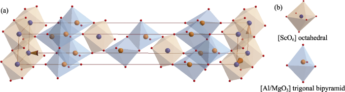
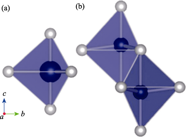
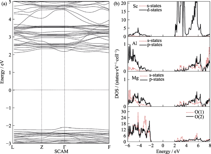
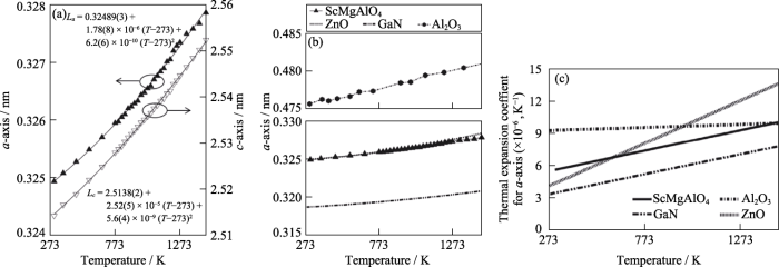
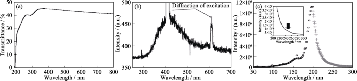
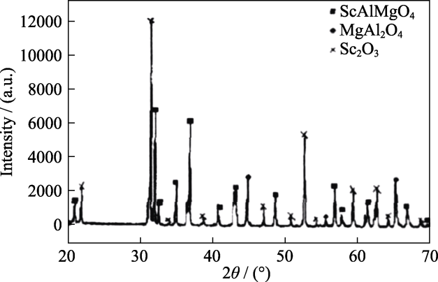
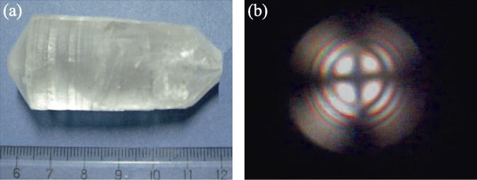
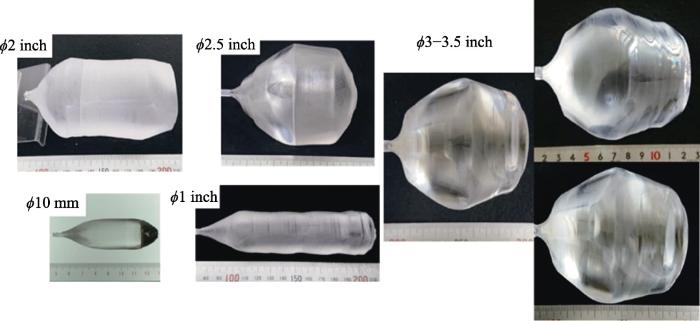
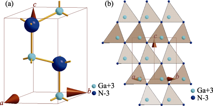
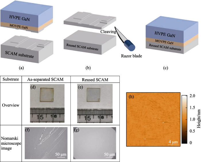
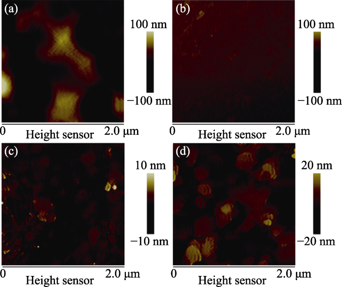
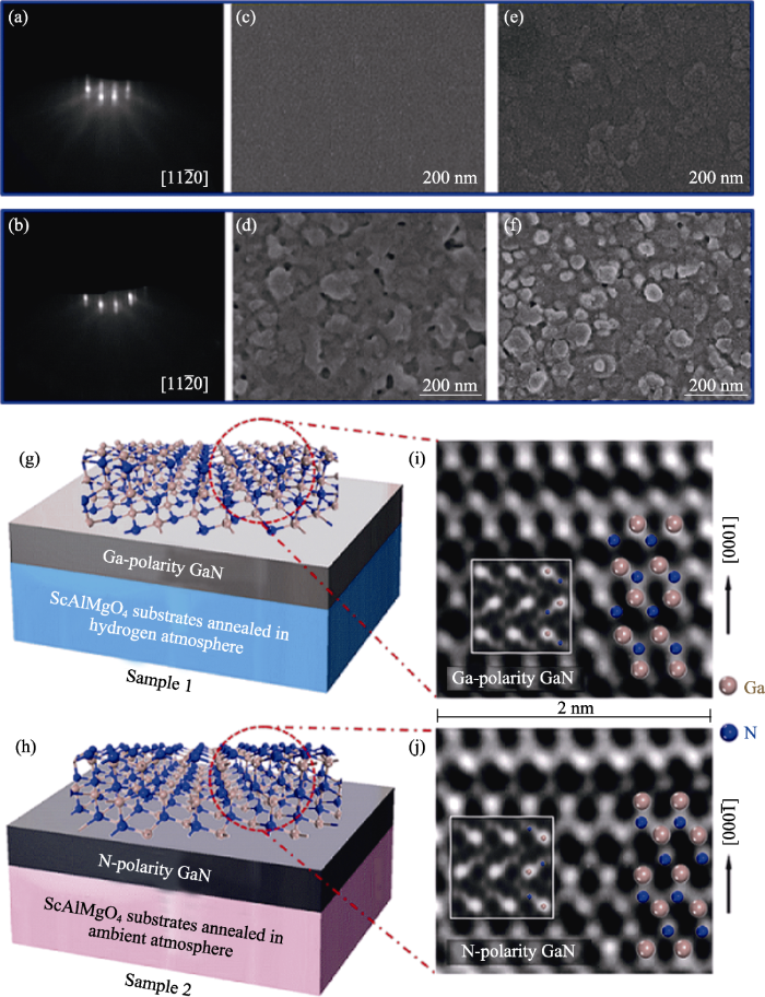

