光探测器根据所产生的载流子的利用方式可以分为光电导型与光伏型[1], 其中光电导型可以根据载流子传输方式分为水平结构与垂直结构[2-3]。光探测器可以将入射光子转换为电信号, 在环境监测、空间探测、生物和图像传感领域应用广泛[4-5]。钙钛矿材料具有极高的光吸收系数、带隙可调性、较长的载流子寿命和扩散长度等优点, 且成本低、易加工, 在光电应用领域中具有广阔的发展空间[6⇓-8]。但是, 钙钛矿材料面临室内环境下稳定性差的问题, 这限制了其进一步发展[9-10]。相比之下, 二维钙钛矿(2D PVK)材料具有更好的热稳定性、化学稳定性以及环境稳定性[11-12], 更适合商业化应用[13-14]。
在层状二维钙钛矿中, 二维卤化铅八面体[PbX6]4-被有机分子分离, 沿垂直方向在范德华力作用下堆积形成堆叠层。首先, 相比于3D, 2D在室温下激子结合能可达到数百MeV, 由于量子限制效应, 2D PVK表现出较强的激子特性[15]。这些光电性质可以增强光学非线性[16], 提高光致发光量子产率。(PEA)2PbI4作为一种常见的2D PVK, 于二十世纪九十年代初问世[17], 具有200 MeV的高激子结合能和约2.36 eV的大带隙, 激子特性明显[18]。其次, 2D具备有机阳离子的疏水性、高度一致的取向和致密的填充特性[19⇓⇓-22], 可以提高PVK表面的耐湿性, 降低晶界密度, 具有良好的稳定性[23-24]。再者, 2D PVK倾向于自主形成量子阱结构, 其中载流子主要集中在无机层[25], 载流子收集是各向异性的, 导致层间输运受到限制[26]。因此, 2D PVK更适用于水平结构的光电探测器, 有利于其收集光生载流子。但水平结构器件电极间距较大, 需要高工作电压维持其较高的增益, 而这由PVK薄膜质量直接决定, 因为在长距离传输过程中, 薄膜的缺陷更容易捕获载流子而加剧光电流的损失[27]。近年来发展的2D无晶界PVK单晶可以有效解决缺陷捕获载流子的问题[28], 但生长单晶过程耗时, 且需要采用高温合成工艺[29]。溶液法成本低、工艺简单, 可用于制备PVK薄膜[30]。如果使用溶液法制备3D PVK薄膜时, 必须引入高温退火来获得所需的PVK相[31]。此外, 为了提高结晶度并减少缺陷[32-33], 往往需要进行添加剂掺杂[34]、反溶剂处理[35]和蒸汽处理[36]等特殊处理。这些方法不适于大规模生产, 因此, 寻找一种简单和低成本的方法来获得高结晶度、高质量的PVK薄膜是当前亟需解决的问题。
本工作以2-苯基乙胺氢碘酸盐(PEAI)和碘化铅(PbI2)为原料, 利用溶液法在低退火温度(80 ℃)条件下、无需特殊处理即可得到高结晶度高质量2D(PEA)2PbI4薄膜, 制备水平光电导型光电探测器, 并系统表征钙钛矿薄膜的结构、形貌和光学性质, 以及光电器件的性能和稳定性。
1 实验方法
1.1 实验试剂
2-苯基乙基胺(C6H5(CH2)2NH2, 99%, Alfa Aesar)溶液、氢碘酸(HI, 45%, 科隆化学)、碘化铅(PbI2, 99.99985%, Alfa Aesar)、N, N-二甲基甲酰胺(DMF, 99.9%, Innochem), 所有试剂均可直接使用, 无需进一步纯化。
1.2 PEAI粉末的合成
将摩尔比为1 : 1的2-苯基乙基胺溶液和氢碘酸溶液加入50 mL的圆底烧瓶, 在0 ℃冰水浴中搅拌反应4 h, 旋蒸至溶剂完全挥发, 再将得到的白色粉末用无水乙醚洗涤三次, 最后将产物置于40 ℃真空干燥烘箱干燥24 h。
1.3 前驱体溶液的制备
在氮气手套箱(CO2<0.01 μL/L, CH2O<0.01 μL/L)中, 将1.2 mmol的PEAI和0.6 mmol的PbI2粉末溶解在1 mL的DMF中, 在室温(23±0.5) ℃下搅拌6 h得到(PEA)2PbI4前驱体溶液。
1.4 光电器件的制备
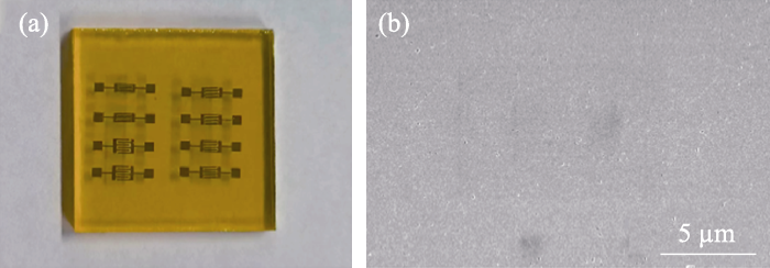
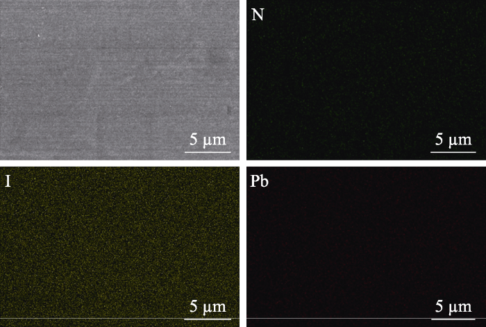
2D (PEA)2PbI4光探测器的器件结构和制备流程如图1(a, b)所示。首先, 在旋涂工艺之前, 使用75%乙醇擦拭裁剪好的2 cm×2 cm的玻璃, 分别在75%乙醇、异丙醇和75%乙醇中超声清洗15 min, 干燥空气吹干后, 使用氧等离子体处理5 min, 以提高亲水性。然后通过蒸镀机采用叉指电极模板热蒸发20 nm厚度的Cu, 得到沟道长度为75 μm、宽度为7000 μm的叉指电极。最后旋涂前驱体溶液, 在滴加前驱体溶液之前, 在玻璃基板上滴加100 μL DMF, 5000 r/min旋涂30 s, 以去除多余的溶液。在80 ℃的热台预热2 min后, 将75 μL (PEA)2PbI4前驱体溶液滴加到玻璃基板上, 采用相同的工艺进行旋涂, 最后在80 ℃的热台上退火5 min, 得到2D (PEA)2PbI4薄膜(图S1(a))。
图1
图1
(a)在玻璃衬底上制备的光电探测器器件结构, (b) (PEA)2PbI4薄膜制备工艺示意图和(c) 80 ℃退火后(PEA)2PbI4薄膜的SEM照片
Fig. 1
(a) Structure of the photodetector device prepared on a glass substrate, (b) schematic diagram of preparation process for the (PEA)2PbI4 thin film, and (c) SEM image of the (PEA)2PbI4 thin film after being annealed at 80 ℃
1.5 测试与表征
采用X射线衍射仪(X-ray Diffraction, XRD, Bruker D2 PHASER, CuKα)分析(PEA)2PbI4薄膜结晶性和晶体结构。采用扫描电子显微镜(Scanning Electron Microscope, SEM, 日立S-4800)表征薄膜和材料的表面形貌。用紫外-可见分光光度计(UV-Vis, 岛津UV-2600型)和荧光光谱仪(Photoluminescence, PL, Pico Quant FluoTime 300)表征样品的光学性能。采用Keithley 2636B系列系统数字源表测试器件的光电性能。
2 结果与讨论
2.1 2D (PEA)2PbI4薄膜的物理性能
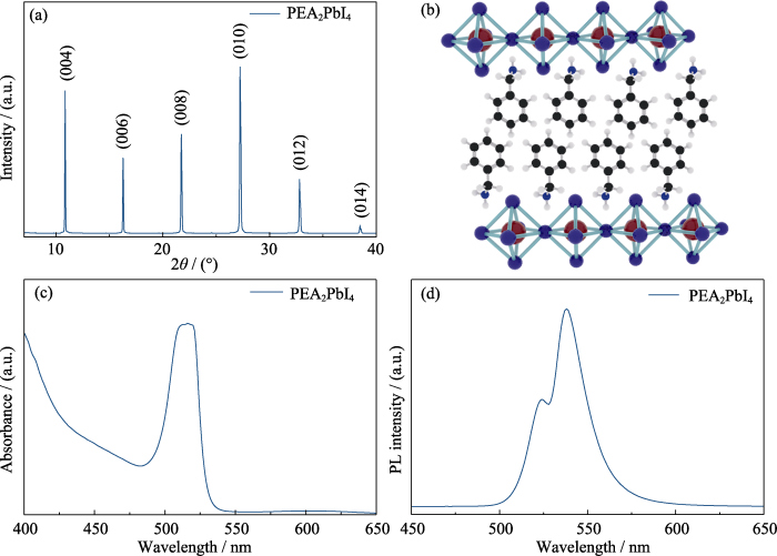
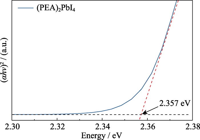
图2(a)为典型的(PEA)2PbI4薄膜的X射线衍射谱图, 其包含一系列明确的周期性分布的衍射峰, 与(00h)(h=4, 6, 8…)晶面相对应[29], 说明薄膜具有较高的结晶度。图S3中DMF预旋涂处理的(PEA)2PbI4薄膜的XRD谱图基本没有变化, 说明预旋涂不会影响钙钛矿的形成过程。图2(b)中(PEA)2PbI4晶体的基本结构单元为经典的二维钙钛矿结构, 两层绝缘的PEA+将[PbX6]4-无机层分开, 有机阳离子层与无机层通过微弱的范德瓦尔斯力彼此相连。(PEA)2PbI4薄膜的吸收光谱(图2(c))中, 唯一的516 nm左右的吸收峰来自PbI4量子阱中的激子, 这说明衬底以及预旋涂DMF都不会影响薄膜的光吸收性能, 吸收截止边在530 nm附近。基于吸收光谱绘制(PEA)2PbI4薄膜的Tauc图((图S4)), 可以计算得到相关的光学带隙为2.357 eV。如图2(d)所示, 薄膜具有两个PL峰, 分别在524和536 nm。此外, 吸收光谱显示出带边截断, 没有吸收尾, 表明通过简单的旋涂工艺制备的(PEA)2PbI4薄膜具有较低的缺陷态密度。
图2
图2
(a)典型的(PEA)2PbI4薄膜的XRD谱图; (b)二维层状(PEA)2PbI4的晶体结构; (PEA)2PbI4薄膜的(c)UV-Vis吸收谱图和(d)PL光谱
Fig. 2
(a) XRD pattern of a typical (PEA)2PbI4 film,(b) crystal structure of two-dimensional layered (PEA)2PbI4, and (c) UV-Vis absorption and (d) PL spectra of (PEA)2PbI4 film
2.2 2D (PEA)2PbI4光电探测器的光电性能
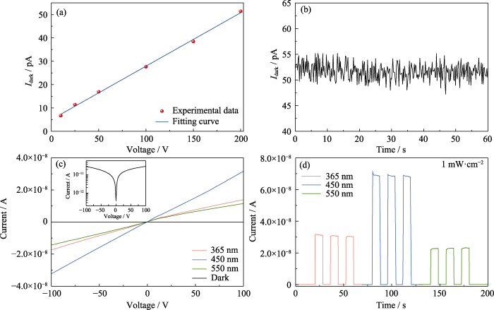
水平光电导型器件与垂直型不同的是: 水平器件电极之间距离较大, 需要施加较高的电压来维持增益[37-38], 但高电压会造成更大的暗电流, 从而直接影响到器件性能[39⇓-41]。含有大量有机阳离子的二维钙钛矿可以有效地抑制缺陷, 降低暗电流[42⇓-44]。图3(a, b)为器件在暗态下的性能, 从图3(a)中可以看出, 当施加电压增加时, 暗电流从初始的~6 pA上升至~53 pA。即使在高电压下, 暗电流仍旧能保持在10-11 A的数量级, 这充分证明成功制备了(PEA)2PbI4高质量薄膜, 缺陷得到有效抑制。此外,最终暗电流不会随时间变化, 一直稳定在一个特定的区间内, 如图3(b)所示。图3(c, d)主要说明器件对不同波长光的选择性。图3(c)是在黑暗下以及不同波长光照下的电流-电压(I-V)曲线, 在光强恒定的条件下, 随着施加电压增大, 光电流快速增大, 说明器件的光响应灵敏度高。重要的是, 该器件对450 nm光的灵敏度明显高于其他两个波长, 这是该器件对不同波长光响应表现出的独特性质。此外, 开关光照下器件电流随时间变化的测试结果如图3(d)所示, 器件的光响应快速、灵敏, 显示出良好的稳定性和可重复性。在固定功率密度为1 mW·cm-2的365、450和550 nm的光照下, 光电流分别增大到30.6、68.8和23.2 nA, 波长为450 nm的光响应最佳, 这与图3(c)的结果吻合。
图3
图3
(PEA)2PbI4光电探测器的(a)暗电流随施加电压的变化曲线, (b)在暗态下暗电流随时间的变化曲线, 在1 mW/cm2光功率密度、不同波长光照下的(c) I-V曲线和(d) I-t曲线
Fig. 3
(a) Dark current versus applied voltage, (b) dark current versus time in the dark state, (c) I-V curves, and (d) I-t curves illuminated at different wavelengths with 1 mW/cm2 for (PEA)2PbI4 photodetector
Colorful figures are available on website
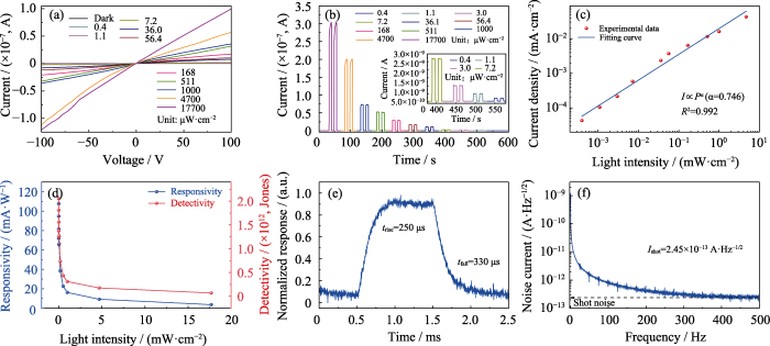
图4(a, b)系统研究了器件对450 nm波长的光响应随光强的变化规律。图4(a)为0.4~ 17.7 mW·cm-2光强范围内的I-V特性。在不同光强度下, (PEA)2PbI4薄膜器件始终表现出典型的欧姆接触。此外, 随着光强增大, 光电流显著增强, 这表明大量光子在器件中产生了更多电子空穴对。图4(b)显示器件具有良好的开关特性, 上升沿和下降沿尖锐, 表明响应速度快。当光强达到17.7 mW·cm-2时, 光电流达到0.31 μA, 计算所得开关比达到5849, 与报道的同类型器件的数值相当[45-46]。根据不同光强的I-t曲线, 绘制了光电流密度(J)与光强(P)的拟合直线, 如图4(c)所示。J与P的对应关系遵循如下规律:
图4
图4
(PEA)2PbI4光电探测器在450 nm不同光强照射下(a) I-V曲线和(b) I-t曲线, (c)在450 nm光照下光电流与光强的拟合直线, (d)在不同光强下的响应度和探测率, (e)响应时间和(f)在不同测试频率下的噪声电流
Fig. 4
(a) I-V and (b) I-t curves illuminated at 450 nm with different light intensities, (c) fitted line of photocurrent vs. light intensity illuminated at 450 nm, (d) responsivities and detectivities at different light intensities, (e) response time and (f) noise currents tested at different frequencies for (PEA)2PbI4 photodetector
Colorful figures are available on website
其中, J为光电流密度, P为光强。通过拟合J-P曲线, 得到α=0.746。α接近于1, 表明制备的(PEA)2PbI4薄膜质量高, 缺陷态密度相对较低。
响应度(R)和探测率(D*)作为评价光电探测器性能的关键参数,可以根据以下公式计算,
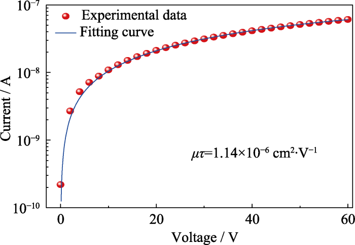
其中, Ilight是光照下的电流(A), Idark是暗电流(A), Pin是激光的入射功率密度(mW/cm2), S是有效感光面积(cm2)。图4(d)给出了不同强度450 nm光照射下的R和D*, 在较低光强(0.4 μW·cm-2)光照下, R和D*随着入射光强的增加而减小, R和D*最高达到107 mA·W-1和2.05×10¹² Jones, 优于已有报道[34], 说明制备的(PEA)2PbI4薄膜具有低缺陷态密度。响应时间也是评价光探测器性能的重要参数, 图4(e)是2D (PEA)2PbI4光电探测器的响应时间, 主要与光生载流子的提取有关。在450 nm的光照下, 该器件的上升时间(trise)和下降时间(tfall)分别为250和330 μs, 响应速度快表明该器件有应用于实时探测的潜力。随后测试了平稳状态下的暗电流, 通过对暗电流进行快速傅里叶变换(FFT), 得到噪声谱密度函数。在图4(f)中看出, (PEA)2PbI4薄膜器件的噪声截止电流Ishot为2.45×10⁻¹³ A·Hz-1/2。噪声电流如此低可以归因于制备得到了高质量薄膜, 薄膜质量越高表面缺陷越少, 传输过程中的载流子散射显著减弱。电荷载流子迁移率(μ)和电荷载流子寿命(τ)的乘积决定了每单位电场的平均载流子漂移距离, 进而影响光电探测器在给定电场下的电荷收集效率。通过光电探测器在450 nm照明下的I-V响应来测量(PEA)2PbI4薄膜器件的μτ乘积。测量的光电流符合Hecht方程:
2.3 2D (PEA)2PbI4光电探测器的稳定性
图5
图5
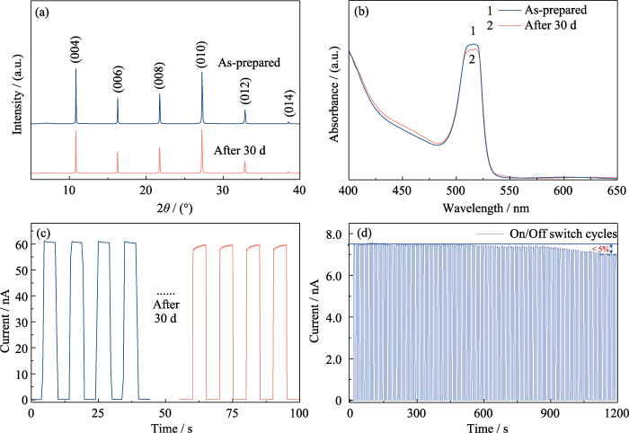
(PEA)2PbI4薄膜和(PEA)2PbI4光电探测器的稳定性
Fig. 5
Stability of the 2D (PEA)2PbI4 film and photodetector
(a) XRD patterns and (b) UV-Vis absorption spectra of (PEA)2PbI4 films before and after laid in the dark and N2 atomsphere for 1 m; (c) I-t curves of (PEA)2PbI4 photodetectors illuminated at 0.5 mW·cm-2 before and after 30 d; (d) I-t curves of the device under continuous illumination of 1200 s
3 结论
综上所述, 本研究报道了一种制备方法简易、成本低的高质量(PEA)2PbI4薄膜以及相应的水平光电导型光探测器。光电探测器具有较低的暗电流(10-11 A), 在450 nm光照下具有良好的响应度(107 mA·W-1)、较高的探测率(2.05×10¹² Jones)和快速响应时间(250 μs/330 μs)。持续控制光照1200 s后, 器件可以保持95%的光电流。此外, 器件静置30 d后光电流几乎保持不变。该器件在高灵敏度光电应用中具有巨大潜力。
补充材料
本文相关补充材料可登录
补充材料
基于二维钙钛矿(PEA)2PbI4的光电探测器
蔡 凯, 靳志文
(兰州大学 物理科学与技术学院, 兰州 730000)
图S1
图S1
(a) (PEA)2PbI4薄膜光电探测器照片; (b) 200 ℃高温退火后的(PEA)2PbI4薄膜的SEM照片
Fig. S1
(a) Picture of a photodetector based on (PEA)2PbI4 film; (b) SEM image of (PEA)2PbI4 film after being annealed at high temperature(200 ℃)
图S2
图S3
图S3
未经过处理与经过DMF预旋涂处理的(PEA)2PbI4薄膜的XRD谱图
Fig. S3
XRD patterns of (PEA)2PbI4 without and with DMF treatment before spin-coating
图S4
图S4
(PEA)2PbI4薄膜的Tauc图, 光学带隙为2.357 eV
Fig. S4
Tauc plot of (PEA)2PbI4 film with an optical band gap of 2.357 eV
图S5
图S5
(PEA)2PbI4薄膜的偏压依赖性光电导
Fig. S5
Bias-dependent photoconductivity of (PEA)2PbI4
图S6
图S6
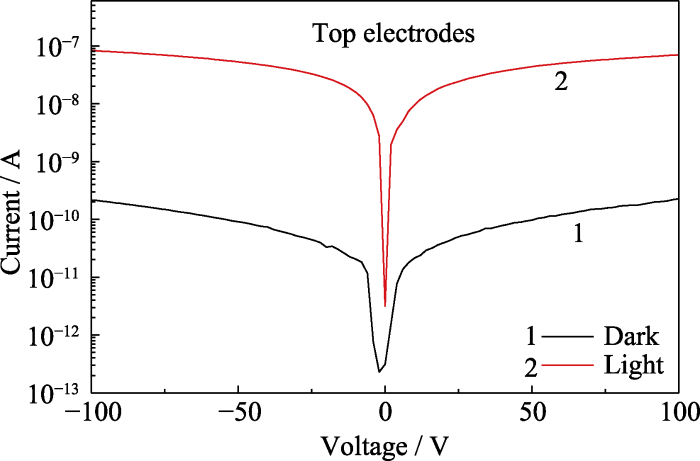
上电极光电探测器在光暗态下的I-V曲线
Fig. S6
I-V curves of photodetector with up-electrode in the light-dark state
参考文献
Emerging perovskite materials with different nanostructures for photodetectors
Opportunities and challenges of inorganic perovskites in high-performance photodetectors
Compared with organic–inorganic hybrid perovskites, fully inorganic perovskites show an increased stability and are therefore attracting considerable attention, especially in recent years. Such materials are not only being extensively used in applications such as solar cells and light-emitting diodes, but also show great potential as photodetectors due to their exceptional optoelectronic properties. In this review, the recent progress on emerging photodetectors based on inorganic perovskites is comprehensively summarized, focusing on the versatile compositions and morphologies of constituent materials and diverse device architectures, and covering the sensing regions from UV–visible–NIR to x-ray and even gamma-ray. A brief outlook that highlights the current challenges impeding the commercialization of inorganic perovskite-based photodetectors is also included, and possible solutions to these problems are provided.
Perovskites Enabled Highly Sensitive and Fast Photodetectors. Perovskite Photovoltaics and Optoelectronics: From Fundamentals to Advanced Applications
Advances in perovskite photodetectors
Asymmetric metal halide film with suppressed leakage current for high sensitive X-ray detection and imaging
Two-dimensional organic- inorganic hybrid Ruddlesden-Popper perovskite materials: preparation, enhanced stability, and applications in photodetection
Photon energy loss and management in perovskite solar cells
Recent progress of scalable perovskite solar cells and modules
Impact of isomers on the photovoltaic properties of polymerized small-molecule acceptors
Interface functionalization in inverted perovskite solar cells: from material perspective
An interface co-modification strategy for improving the efficiency and stability of CsPbI3 perovskite solar cells
2D Dion-Jacobson CsPbI3 with enhanced interlayer coupling for stable and efficient photovoltaics
Recent advances in perovskite/2D materials based hybrid photodetectors
Since 2009, metal halide perovskites have attracted a great deal of attention in different optoelectronic applications, such as solar cells, photodetectors (PDs), light-emitting diodes, lasers etc, owing to their excellent electrical and optoelectrical properties. However, since the discovery of graphene, atomically thin 2D materials have been the central focus of materials research due to its exciting properties. Thus, integrating 2D materials with perovskite material can be highly promising for various optoelectronic applications, in particular for ultrasensitive photodetection. In these PDs, 2D materials serve various roles, such as charge transport layer, Schottky contacts, photo absorbers, etc, while perovskite is the light-harvesting active layer. In this review, we focus on the recent findings and progress on metal halide perovskite/2D material phototransistors and hybrid PDs. We comprehensively summarize recent efforts and developments of perovskite/graphene, perovskite/transition-metal dichalcogenides, perovskite/black phosphorus, and perovskite/MXene based phototransistor and heterojunction PDs from the perspective of materials science and device physics. The perovskite/2D material phototransistor can exhibit very high photoresponsivity and gain due to the amplification function of transistors and the pronounced photogating effect in 2D material, while perovskite/2D material heterojunction PD can operate without external bias due to built-in potential across the heterojunction. This review also provides state-of-the-art progress on flexible, transparent, self-powered and PD systems and arrays based on perovskite/2D materials. After summarizing the ongoing research and challenges, the future outlook is presented for developing metal halide perovskite/2D material hybrid PDs for practical applications.
Progress and prospects of two-dimensional materials for membrane-based osmotic power generation
Enhancing two-dimensional perovskite photodetector performance through balancing carrier density and directional transport
A balance between carrier density and carrier directional transport is achieved when the inorganic layer number n is 4, and thereby a high-efficiency perovskite single crystal horizontal photodetector is prepared.
Image charge effect on two-dimensional excitons in an inorganic-organic quantum- well crystal
Self-organized growth of PbI-based layered perovskite quantum well by dual-source vapor deposition
Fine coverage and uniform phase distribution in 2D (PEA)2Cs3Pb4I13 solar cells with a record efficiency beyond 15%
Manipulate energy transport via fluorinated spacers towards record-efficiency 2D Dion-Jacobson CsPbI3 solar cells
Fluorosubstitution boosting 2D Ruddlesden-Popper CsPbI3 with high stability and efficiency
Novel PHA organic spacer increases interlayer interactions for high efficiency in 2D Ruddlesden- Popper CsPbI3 solar cells
A novel multiple-ring aromatic spacer based 2D Ruddlesden-Popper CsPbI3 solar cell with record efficiency beyond 16%
Engineering strategies for two-dimensional perovskite solar cells
Advancing 2D perovskites for efficient and stable solar cells: challenges and opportunities
Highly sensitive X-ray detector made of layered perovskite-like (NH4)3Bi2I9 single crystal with anisotropic response
Sensitive and stable 2D perovskite single-crystal X-ray detectors enabled by a supramolecular anchor
Perovskite-based photodetectors: materials and devices
While the field of perovskite-based optoelectronics has mostly been dominated by photovoltaics, light-emitting diodes, and transistors, semiconducting properties peculiar to perovskites make them interesting candidates for innovative and disruptive applications in light signal detection. Perovskites combine effective light absorption in the broadband range with good photo-generation yield and high charge carrier mobility, a combination that provides promising potential for exploiting sensitive and fast photodetectors that are targeted for image sensing, optical communication, environmental monitoring or chemical/biological detection. Currently, organic-inorganic hybrid and all-inorganic halide perovskites with controlled morphologies of polycrystalline thin films, nano-particles/wires/sheets, and bulk single crystals have shown key figure-of-merit features in terms of their responsivity, detectivity, noise equivalent power, linear dynamic range, and response speed. The sensing region has been covered from ultraviolet-visible-near infrared (UV-Vis-NIR) to gamma photons based on two- or three-terminal device architectures. Diverse photoactive materials and devices with superior optoelectronic performances have stimulated attention from researchers in multidisciplinary areas. In this review, we provide a comprehensive overview of the recent progress of perovskite-based photodetectors focusing on versatile compositions, structures, and morphologies of constituent materials, and diverse device architectures toward the superior performance metrics. Combining the advantages of both organic semiconductors (facile solution processability) and inorganic semiconductors (high charge carrier mobility), perovskites are expected to replace commercial silicon for future photodetection applications.
Perovskite-type 2D materials for high-performance photodetectors
Surface-tension-controlled crystallization for high-quality 2D perovskite single crystals for ultrahigh photodetection
A review on solution-processed perovskite/organic hybrid photodetectors
Spontaneous low-temperature crystallization of alpha-FAPbI3 for highly efficient perovskite solar cells
High-performance large-area perovskite photovoltaic modules
Self-assembled monolayer enabling improved buried interfaces in blade-coated perovskite solar cells for high efficiency and stability
Wavelength selective and cesium halides additive photodetectors based on two-dimensional perovskite: (C8H9NH3)2PbBr4
One-step anti-solvent associated method for high performance two-dimensional perovskite photodetectors fabrication at low temperature
Realizing a highly luminescent perovskite thin film by controlling the grain size and crystallinity through solvent vapour annealing
Inhibition of ion migration for reliable operation of organolead halide perovskite- based metal/semiconductor/metal broadband photodetectors
Organohalide lead perovskite based photodetectors with much enhanced performance
Research progress of high- sensitivity perovskite photodetectors: a review of photodetectors: noise, structure, and materials
Solution-processed perovskite crystals for electronics: moving forward
Visualization of carrier transport in lateral metal-perovskite-metal structures and its influence on device operation
Polarization-driven self-powered photodetection in a single-phase biaxial hybrid perovskite ferroelectric
Tailored engineering of an unusual (C4H9NH3)2(CH3NH3)2Pb3Br10 two-dimensional multilayered perovskite ferroelectric for a high-performance photodetector
Heterogeneous nucleation of crystals from vapor
A rate equation is derived for heterogeneous nucleation of crystals from the vapor on the basis of an adsorption, surface diffusion, and statistical fluctuation mechanism. It should be emphasized that the term surface diffusion as used in this development does not imply the existence of a gradient. Rather it refers to random movement of absorbed atoms on the subtrate surface. It is shown that this mechanism results in a rate at least 102 to 103 times greater than that calculated on the basis of direct addition of atoms to the critical nucleus from the vapor phase. The equation describes the temperature dependence of existing critical supersaturation data for heterogeneous nucleation. Analysis of the existing data by this treatment permits an evaluation of the standard free energy of adsorption. Particular attention is given to heterogeneous nucleation from atomic beams.
Mixed-dimensional self-assembly organic-inorganic perovskite microcrystals for stable and efficient photodetectors
Semi-transparent, high-performance lead-free Cs3Bi2I9 single crystal self-driven photodetector
All-inorganic Bi-based perovskites have attracted much attention due to their excellent stability, environmentally friendly, and low-cost solution processability. However, due to the large exciton binding energy and small light absorption coefficient, the performance of the Bi-based perovskite photodetector (PD) is far behind of the traditional Pb-based perovskite PDs. In this work, the lead-free all-inorganic Cs3Bi2I9 (CBI) perovskite single crystal was synthesized by a space-confined antisolvent-assisted crystallization method for high-performance, semi-transparent, and self-driven PDs with an ITO/SnO2/CBI/PTAA/Au/ITO structure. Electrical and optical properties of Au/ITO transparent electrode were studied considering its figure of merit and device quantum efficiency through optimizing the Au thickness. Finally, our optimized semi-transparent device showed excellent self-driven performance with a large on/off ratio of ∼5700, a high responsivity of 52.06 mA/W, a high detectivity of >1012 Jones, and a large linear dynamic range of up to 140.7 dB. In addition, our device demonstrated excellent characteristics to the weak light detection and the long-term stability. The Au/ITO electrode was adopted and tailored to balance the device performance and transparency, which provides a good route for developing high-performance and transparent devices in the future.


