外场下NBT-KBT100
 , 郑学军, 张丹书
 Domain Switching, Retention and Imprint of NBT-KBT100
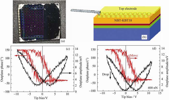
Fig. 6 The NBT-KBT17 thin film surface morphology plated with top electrode observed by metallographic microscope a, capacitor structure schematic b, the phase and amplitude-electric voltage hysteresis loops of ferroelectric capacitor before c and after stressing d
