Journal of Inorganic Materials ›› 2021, Vol. 36 ›› Issue (6): 608-614.DOI: 10.15541/jim20200509
• RESEARCH ARTICLE • Previous Articles Next Articles
CHEN Lichi1,2( ), WANG Yaogong1,2, WANG Wenjiang1,2, MA Xiaoqin1,2, YANG Jingyuan3(
 ), ZHANG Xiaoning1,2
Received:2020-09-01
Revised:2020-10-12
Published:2021-06-20
Online:2020-12-01
Contact:
YANG Jingyuan, engineer. E-mail: yjytonghu@163.com
About author:CHEN Lichi(1995-), male, PhD candidate. E-mail: 734167430@qq.com
Supported by:CLC Number:
CHEN Lichi, WANG Yaogong, WANG Wenjiang, MA Xiaoqin, YANG Jingyuan, ZHANG Xiaoning. Preparation of Silicon Nanowires and Porous Silicon Composite Structure by Electrocatalytic Metal Assisted Chemical Etching[J]. Journal of Inorganic Materials, 2021, 36(6): 608-614.

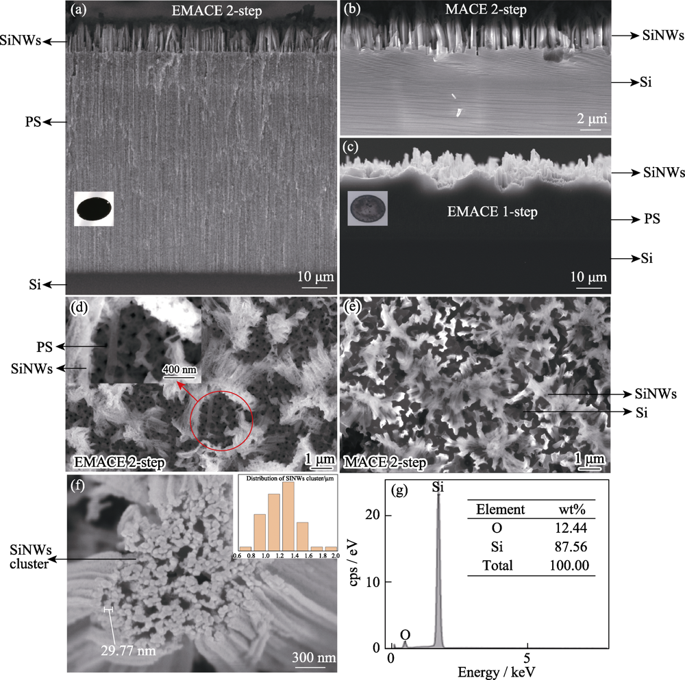
Fig. 2 SEM morphologies of samples prepared by different methods (a,d) EMACE 2-step method; (b,e) MACE 2-step method; (c) EMACE 1-step method; (f) High resolusion FESEM images of SiNWs clusters; (g) EDS of SiNWs clusters

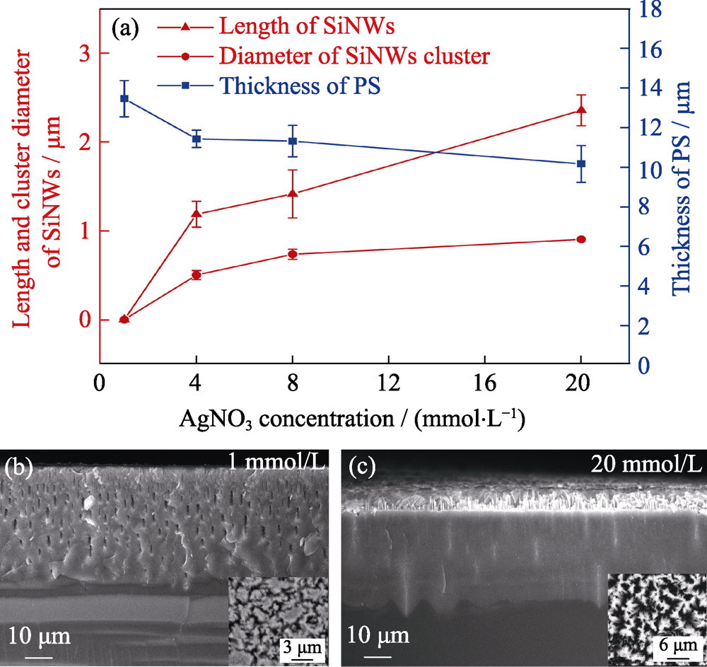
Fig. 3 Effect of AgNO3 concentration on the morphology of SiNWs/PS composites (a) Changes of length of SiNWs, PS and cluster with AgNO3 concentration, and FESEM images of SiNWs/PS composites with AgNO3 concentration of (b) 1 mmol/L and (c) 20 mmol/L

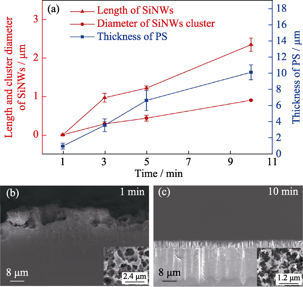
Fig. 4 Effect of etching time on the morphology of SiNWs/PS composites (a) Changes of length of SiNWs, PS and cluster with etching time, and FESEM images of SiNWs/PS composites with etching time of (b) 1 min and (c) 20 min

Fig. 8 Variation of voltage/current between anode and cathode with time during the etching (a) EMACE 2-step method at 10 mA; (b) EMACE 2-step method at 30 mA; (c) EMACE 1-step method at 10 mA
| [1] |
PIEDIMONTE P, MAZZETTA I, FUCILE S, et al. Silicon nanowires to detect electric signals from living cells. Materials Research Express, 2019,6(8):084005.
DOI URL |
| [2] |
DIMAGGIO E, PENNELLI G. Potentialities of silicon nanowire forests for thermoelectric generation. Nanotechnology, 2018,29(13):135401.
DOI URL |
| [3] |
PENNELLI G, ELYAMNY S, DIMAGGIO E, et al. Thermal conductivity of silicon nanowire forests. Nanotechnology, 2018,29(50):505402.
DOI URL |
| [4] |
MOKSHIN P V, JUNEJA S, PAVELYEV V S. Synthesis of silicon nanowires using plasma chemical etching process for solar cell applications. Journal of Physics: Conference Series, 2019,1368(2):022060.
DOI URL |
| [5] |
CHEN W H, CABARROCAS P R I. Rational design of nanowire solar cells: from single nanowire to nanowire arrays. Nanotechnology, 2019,30(19):194002.
DOI URL |
| [6] |
KUMAR V, SAXENA S K, KAUSHIK V, et al. Silicon nanowires prepared by metal induced etching (MIE): good field emitters. RSC Advances, 2014,4(101):57799-57803.
DOI URL |
| [7] |
ADAM T, HASHIM U. Silicon nanowire fabrication: silicon trimming via shallow anisotropic etching. Microelectronics International, 2014,31(2):78-85.
DOI URL |
| [8] |
ACHARYA S, KOTTANTHARAYIL A. Poole-Frenkel transport in gold catalyzed VLS grown silicon nanowires. IEEE Transactions on Electron Devices, 2018,65(5):1685-1691.
DOI URL |
| [9] |
LESTER U VINZONS, LEI SHU, SENPO YIP, et al. Unraveling the morphological evolution and etching kinetics of porous silicon nanowires during metal-assisted chemical etching. Nanoscale Research Letters, 2017,12:385.
DOI URL |
| [10] |
CONG L T, NGOC LAM N T, GIANG N T, et al. N-type silicon nanowires prepared by silver metal-assisted chemical etching: fabrication and optical properties. Materials Science in Semiconductor Processing, 2019,90:198-204.
DOI URL |
| [11] |
VIRIDIANA ACA-LÓPEZ, ENRIQUE QUIROGA-GONZÁLEZ, ESTELA GÓMEZ-BAROJAS, et al. Effects of the doping level in the production of silicon nanowalls by metal assisted chemical etching. Materials Science in Semiconductor Processing, 2020,118:105206.
DOI URL |
| [12] |
ZHU Y F, ZHOU L, PAN C J, et al. Fabrication of silicon nanorod arrays via a facile metal-assisted chemical etching method. Journal of Materials Science Materials in Electronics, 2016,27(6):5833-5838.
DOI URL |
| [13] |
HUNG Y J, LEE S L. Manipulating the antireflective properties of vertically-aligned silicon nanowires. Solar Energy Materials & Solar Cells, 2014,130:573-581.
DOI URL |
| [14] |
LI L, FANG Y, XU C, et al. Fabricating vertically aligned sub-20 nm Si nanowire arrays by chemical etching and thermal oxidation. Nanotechnology, 2016,27(16):165303.
DOI URL |
| [15] |
HE LI, WANG WEN-JIANG, ZHANG XIAO-NING. Improvement of electron emission characteristics of porous silicon emitter by using cathode reduction and electrochemical oxidation. Applied Surface Science, 2017,399:592-598.
DOI URL |
| [16] |
KOMODA T, SHENG X, KOSHIDA N. Mechanism of efficient and stable surface-emitting cold cathode based on porous polycrystalline silicon films. Journal of Vacuum Science & Technology B, 1999,17(3):1076-1079.
DOI URL |
| [17] |
FENG W, ARAKI H, OZAKI M, et al. Field emission properties of the nonaligned multiwalled carbon nanotube films with different length. Japanese Journal of Applied Physics, 2005,44(1-7):L253-L255.
DOI URL |
| [18] |
ZHU K, VINZANT T B, NEALE N R, et al. Removing structural disorder from oriented TiO2 nanotube arrays: reducing the dimensionality of transport and recombination in dye-sensitized solar cells. Nano Letters, 2007,7(12):3739.
DOI URL |
| [19] |
HAN H, HUANG Z, LEE W. Metal-assisted chemical etching of silicon and nanotechnology applications. Nano Today, 2014,9(3):271-304.
DOI URL |
| [20] |
ABDULKADIR A, AZIZ A, PAKHURUDDIN M Z. Effects of silver nanoparticles layer thickness towards properties of black silicon fabricated by metal-assisted chemical etching for photovoltaics. SN Applied Sciences, 2020,2(4):515.
DOI URL |
| [21] |
ALHER M A, MOSLEH A, BANIHASHEMIAN S F. Investigation of silicon nanowires produced by metal-assisted chemical etching method. IOP Conference Series: Materials Science and Engineering, 2020,671(1):012028.
DOI URL |
| [22] |
CULLIS A G, CANHAM L T, CALCOTT P J. The structural and luminescence properties of porous silicon. Journal of Applied Physics, 1997,82(3):909-965.
DOI URL |
| [23] | FOWLER R H, NORDHEIM L. Electron emission in intense electric fields. Proceedings of the Royal Society of London, 1928,119(781):173-181. |
| [1] | LI Kunru, HU Xinghui, ZHANG Zhengfu, GUO Yuzhong, HUANG Ruian. Three-dimensional Porous Biogenic Si/C Composite for High Performance Lithium-ion Battery Anode Derived from Equisetum Fluviatile [J]. Journal of Inorganic Materials, 2021, 36(9): 929-935. |
| [2] | DING Sheng, NING Kai, YUAN Binxia, PAN Weiguo, YIN Shibin, LIU Jianfeng. Durability of Fe-N/C Catalysts with Different Nanostructures for Electrochemical Oxygen Reduction in Alkaline Solution [J]. Journal of Inorganic Materials, 2020, 35(8): 953-958. |
| [3] | ZHANG Tong,LI Zi-Juan,GUO Ze-Kun,TIAN Yan,LIN Hao-Jian,XU Ning-Sheng,CHEN Jun,DENG Shao-Zhi,LIU Fei. Single Crystalline SmB6 Nanostructure Arrays: Controllable Synthesis and Field Emission Property [J]. Journal of Inorganic Materials, 2020, 35(2): 199-204. |
| [4] | SHENG Peng, ZHAO Guang-Yao, XU Li, LIU Shuang-Yu, WANG Bo, LIU Hai-Zhen, MA Guang, HAN Yu, CHEN Xin. Reductive Preparation of Blue TiO2 via Deposition of Aluminum [J]. Journal of Inorganic Materials, 2018, 33(9): 942-948. |
| [5] | ZHOU Hui, HAN Man-Gui, TANG Zhong-Kai, WU Yan-Hui. Fabrication and Magnetic Properties of N-type Porous Silicon/Nickel Microtubes Composite [J]. Journal of Inorganic Materials, 2016, 31(8): 855-859. |
| [6] | WANG Ya-Peng, LIU Jia-Jia, LIU Chun-Xiao, CHEN Wei-Wei, LI Ting-Ting, GUO Hong. Morphology-controlled Synthesis of Hollow Core-shell Structural α-MoO3-SnO2 with Superior Lithium Storage [J]. Journal of Inorganic Materials, 2015, 30(9): 919-924. |
| [7] | ZHAO Peng, LI Zhong, CUI Xiao-Li. Facile Preparation Carbon-Doped TiO2 Nanotube Electrodes and Its Enhanced Photoelectrochemical Response [J]. Journal of Inorganic Materials, 2015, 30(6): 599-604. |
| [8] | YE Zuo-Yan, LIU Dao-Xin, LI Chong-Yang, ZHANG Xiao-Hua, ZANG Xiao-Ming, LEI Ming-Xia. Effect of Sealing Treatments on the Corrosion Behavior of Micro-arc Oxidation Coating on Aluminum Alloy in Acid NaCl Solution [J]. Journal of Inorganic Materials, 2015, 30(6): 627-632. |
| [9] | HUANG Yan-Hua, HAN Xiang, CHEN Hui-Xin, CHEN Song-Yan, YANG Yong. Investigation of Porous Silicon/Carbon Composite as Anodes for Lithium Ion Batteries [J]. Journal of Inorganic Materials, 2015, 30(4): 351-356. |
| [10] | LU Yuan, YANG Jian-Feng, LI Jing-Long. Fabrication of Porous Silicon Nitride with High Porosity by Carbothermal Reduction-reaction Bonding [J]. Journal of Inorganic Materials, 2013, 28(5): 469-473. |
| [11] | YE Yun, CHEN Tian-Yuan, CAI Shou-Jin, YAN Min, LIU Yu-Hui, GUO Tai-Liang. Effects of Different Humidity on the Growth and Field Emission Properties of CuO Nanowires [J]. Journal of Inorganic Materials, 2013, 28(12): 1359-1363. |
| [12] | LI Jian-Wen, ZHOU Ai-Jun, LIU Xing-Quan, LI Jing-Ze. Si Nanowire Anode Prepared by Chemical Etching for High Energy Density Lithium-ion Battery [J]. Journal of Inorganic Materials, 2013, 28(11): 1207-1212. |
| [13] | CHEN Yu, LI Wen-Rui, XU Can, SU Jia-Can, LI Ming, LIU Chang-Sheng. Study on Hemostatic Materials of Mesoporous Silicon Dioxide Doped Ca and Ag with Antibacterial Properties [J]. Journal of Inorganic Materials, 2012, 27(5): 513-518. |
| [14] | YAO Dong-Xu,ZENG Yu-Ping. High Flexural Strength Porous Silicon Nitride Prepared via Nitridation of Silicon Powder [J]. Journal of Inorganic Materials, 2011, 26(4): 422-426. |
| [15] | ZHANG Zhi-Yu, SANG Li-Xia, LU Li-Ping, BAI Guang-Mei, DU Chun-Xu, MA Chong-Fang. Preparation of TiO2 Nanotube Arrays and Their Photoelectrochemical Properties [J]. Journal of Inorganic Materials, 2010, 25(11): 1145-1149. |
| Viewed | ||||||
|
Full text |
|
|||||
|
Abstract |
|
|||||