
Journal of Inorganic Materials ›› 2019, Vol. 34 ›› Issue (9): 1004-1010.DOI: 10.15541/jim20180584
• RESEARCH LETTERS • Previous Articles Next Articles
TAO You-Rong,CHEN Jin-Qiang,WU Xing-Cai( )
)
Received:2018-12-14
Published:2019-09-20
Online:2019-05-13
Supported by:CLC Number:
TAO You-Rong,CHEN Jin-Qiang,WU Xing-Cai. Phototransistor Based on Single TaON Nanobelt and Its Photoresponse from Ultraviolet to Near-infrared[J]. Journal of Inorganic Materials, 2019, 34(9): 1004-1010.
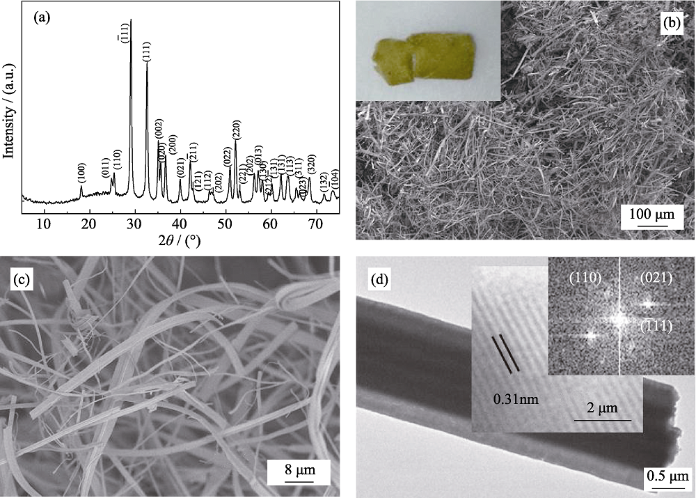
Fig. 1 (a) XRD pattern, (b) low-magnification SEM image (inset: light photograph), and (c) high-magnification SEM image of TaON nanobelts; (d) TEM image of a single TaON nanobelt with inset in the middle showing corresponding HRTEM image, and inset on the upper right corner showing FFT pattern of HRTEM image
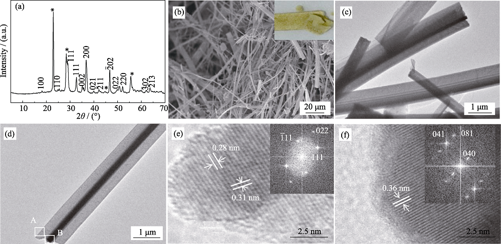
Fig. 2 (a) XRD pattern (a peak with star representing Ta2O5, and the rest peaks representing TaON), (b) low-magnification SEM image (inset: light photograph), and (c) TEM image of Ta2O5@TaON composite nanobelts; (d) TEM image of a single Ta2O5@TaON nanobelt; (e, f) HRTEM images of square A and B in (d), respectively with insets showing FFT patterns of corresponding HRTEM images
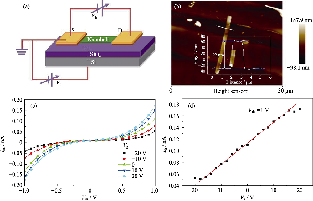
Fig. 3 (a) Scheme of FET based on a single TaON nanobelt; (b) Overlooked AFM image of the FET with inset showing size profile of the nanobelt; (c) Ids-Vds plots at different Vg; (d) Ids-Vg plot at Vds= 1 V
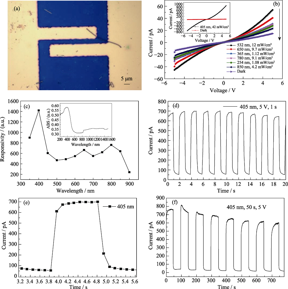
Fig. 4 (a) Photograph of a single TaON nanobelt FET, (b) I-V characteristics of the FET illuminated and unilluminated with different wavelength light, (c) responsivities of the FET to different wavelengths with inset showing UV-Vis absorption spectrum of TaON NBs, (d, f) transient photoresponses of the FET illuminated by 405 nm (42 mW/cm2) light pulse chopped with a photoswitch period of 1 and 50 s at bias of 5 V and (e) local magnification of (d) from 3.2 s to 5.6 s
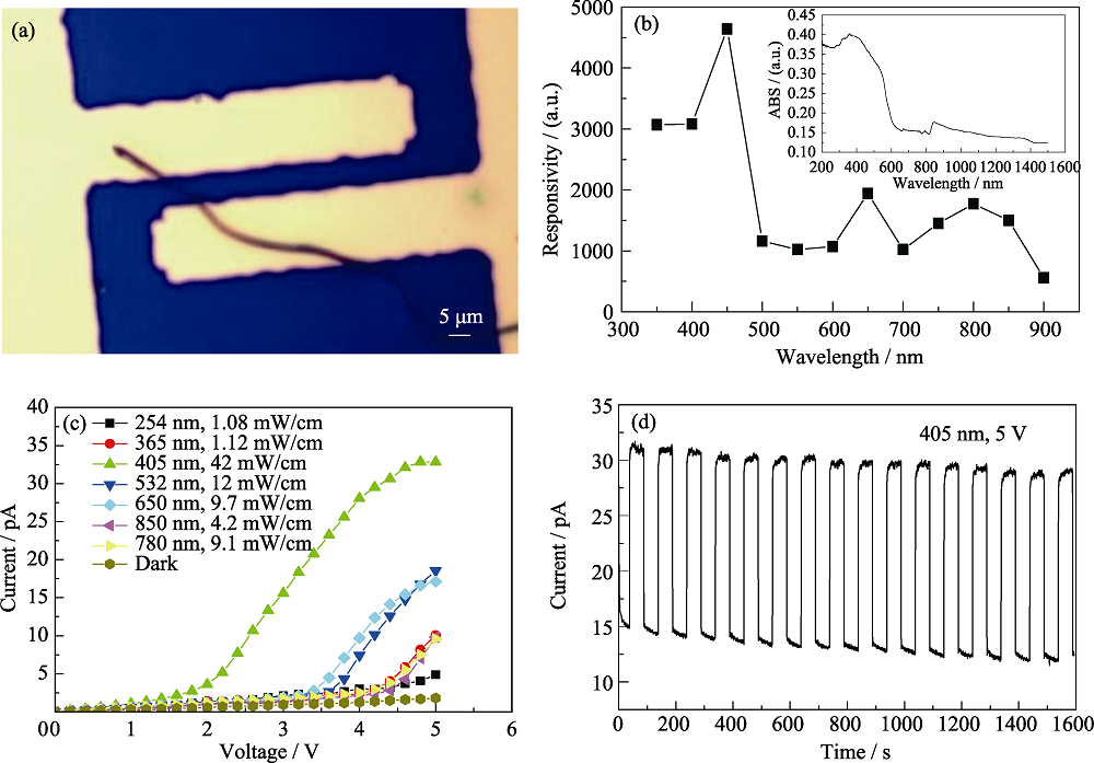
Fig. 5 (a) Photography of FET based on a single Ta2O5@TaON nanobelt, (b) photoresponsivities of the FET to different wavelengths with inset showing UV-Vis absorption spectrum of Ta2O5@TaON NBs, (c) I-V characteristics of the FET unilluminated illuminated with different wavelength light, and (d) transient responses of the FET illuminated with a 405 nm (42 mW/cm2) light pulse chopped with a photoswitch period of 50 s at a bias voltage of 5 V
| Photodetector | Wavelength/Power | Bias voltage/V | Rl/(A·W-1) | Photoswitch current ratio | Rise time/ Decay time | Ref. |
|---|---|---|---|---|---|---|
| CdTe NB | 400 nm/637 mW·cm-2 | 10 | 12 | 1.1 | ~1.1s/~3.3 s | [27] |
| Single-layer MoS2 | 550 nm/80 mW | 1 | 4.2′10-4 | <0.05 s | [28] | |
| GaS NB | 490 nm/0.5 mW·cm-2 | 2 | 2.3′10-3 | <0.03 s | [29] | |
| ZrS3 NB | 405 nm/10.5 mW·cm-2 | 5 | 3.9 | 13 | <0.4 s | [6] |
| Ta3N5 NB | 450 nm/2.8 mW·cm-2 | 2 | 99.6 | ~1.5 | ~45 ms/40 ms | [24] |
| TaON NB | 405 nm/ 42 mW·cm-2 | 5 | 0.249 | 11 | <0.2 s | This work |
| Ta2O5@TaON NB | 405 nm/ 42 mW·cm-2 | 5 | 3.9×10⁻³ | 2 | <0.2 s | This work |
| [1] | GLUSCHKE J G, SEIDL J, BURKE A M , , et al. Achieving short high-quality gate-all-around structures for horizontal nanowire fieldeffect transistors. Nanotechnology, 2019, 30(6): 064001-1-7. |
| [2] | LIANG J R, ZHAO Y R, ZHU K L ,et al. Synthesis and room temperature NO2 gas sensitivity of vanadium dioxide nanowire structures by chemical vapor deposition. The Solid Films, 2019,669:537-543. |
| [3] | ZHANG Y L, WU X C, TAO Y R , et al. Fabrication and field-emission performance of zirconium disulfide nanobelt arrays. Chemical Communications, 2008(23):2683-2685. |
| [4] | WU X C, HONG J M, TAO Y R ,et al. Controlled growth and field-emission properties of NbSe2 micro/nanostructured films. Journal of Nanoscience and Nanotechnoloy, 2010,10(10):6465-6472. |
| [5] | TAO Y R, WU X C, XIONG W W . Flexible visible-light photodetectors with broad photoresponse based on ZrS3 nanobelt films. Small, 2014,10(23):4905-4911. |
| [6] | TAO Y R, WU J J, WU X C . Enhanced ultraviolet-visible light responses of phototransistors based on single and a few ZrS3 nanobelts. Nanoscale, 2015,7(34):14292-14298. |
| [7] | TIAN W, ZHANG C, ZHAI T Y ,et al. Flexible ultraviolet photodetectors with broad photoresponse based on branched ZnS-ZnO heterostructure nanofilms. Advanced Materials, 2014,26(19):3088-3093. |
| [8] | VETTORI M, PIAZZA V, CATTONI A , , et al. Growth optimization and characterization of regular arrays of GaAs/AlGaAs core/shell nanowires for tandem solar cells on silicon. Nanotechnology, 2019, 30(8): 08400-1-15. |
| [9] | GU S S, LOU Z, MA X D ,et al. CuCo2O4 nanowires grown on a Ni wire for high-performance flexible fiber supercapacitors. ChemElectroChem, 2015,2(7):1042-1047. |
| [10] | PENG L, HU L F, FANG X S . Low-dimensional nanostructure ultraviolet photodetectors. Advanced Materials, 2013,25(37):5321-5328. |
| [11] | GONG X, TONG M H, XIA Y J ,et al. High-detectivity polymer photodetectors with spectral response from 300 nm to 1450 nm. Science, 2009,325(5948):1665-1667. |
| [12] | BORUAH B D, MUKHERJEE A, MISRA A . Sandwiched assembly of ZnO nanowires between graphene layers for a self-powered and fast responsive ultraviolet photodetector. Nanotechnology, 2016, 27(9): 095206-1-11. |
| [13] | ZHAO Y M, FENG S L, JIANG H T ,et al. Catalyst-free growth of a Zn2GeO4 nanowire network for high-performance transfer-free solar-blind deep UV detection. Physica E-Low-Dimensional Systems Nanostructures, 2019,107:1-4. |
| [14] | GERTMAN R, HARUSH A, VISOLY-FISHER I . Nanostructured photocathodes for infrared photodetectors and photovoltaics. Journal of Physical Chemistry C, 2015,119(4):1683-1689. |
| [15] | WU J J, TAO Y R, WU Y ,et al. Ultrathin SnS2 nanosheets of ultrasonic synthesis and their photoresponses from ultraviolet to near-infrared. Sensor and Actuators B-Chemical, 2016,231:211-217. |
| [16] | HAFEEZ M, GAN L, LI H Q ,et al. Large-area bilayer ReS2 film/multilayer ReS2 flakes synthesized by chemical vapor deposition for high performance photodetectors. Advanced Functional Materials, 2016,26(25):4551-4560. |
| [17] | XIONG W W, CHEN J Q, WU X C ,et al. Visible light detectors based on individual ZrSe3 and HfSe3 nanobelts. Journal of Materials Chemistry C, 2015,3(9):1929-1934. |
| [18] | TAO Y R, CHENJ Q, WU J J , et al. Flexible ultraviolet-visible photodetector based on HfS3 nanobelt film. Journal of Alloys and Compounds, 2016,658:6-11. |
| [19] | CHUN W J, ISHIKAWA A, FUJISAWA H ,et al. Conduction and valence band positions of Ta2O5, TaON, and Ta3N5 by UPS and electrochemical methods. Journal of Physical Chemistry B, 2003,107(8):1798-1803. |
| [20] | BERTAUX S, REYNDERS P, HEINTZ J M ,et al. New (oxy) nitride pearlescent pigments. Materials Science Engineering B, 2005,121(1/2):137-144. |
| [21] | CHEN S S, QI Y, HISATOMI T ,et al. Efficient visible-light-driven Z-scheme overall water splitting using a MgTa2O6-xNy/TaON heterostructure photocatalyst for H2 evolution. Angewandte Chemie International Edition, 2015,54(29):8498-8501. |
| [22] | ITO S, THAMPI K P, COMTE P , et al. Highly active meso- microporous TaON photocatalyst driven by visible light. Chemical Communications, 2005(2):268-270. |
| [23] | NAKAMURA R, TANAKA T, NAKATO Y . Oxygen photoevolution on a tantalum oxynitride photocatalyst under visible-light irradiation: how does water photooxidation proceed on a metal- oxynitride surface? Journal of Physical Chemistry B, 2005,109(18):8920-8927. |
| [24] | WU X C, TAO Y R, LI L ,et al. Centimeter-long Ta3N5 nanobelts: synthesis, electrical transport, and photoconductive properties. Nanotechnology, 2013,24(17):175701. |
| [25] | WU X C, TAO Y R, GAO Q X , et al. Superconducting TaS2-xIy hierarchical nanostructures. Chemical Communications, 2009(28):4290-4292. |
| [26] | WU X C, TAO Y R, GAO Q X . Fabrication of TaS2 nanobelt arrays and their enhanced field-emission. Chemical Communications, 2009(40):6008-6010. |
| [27] | XIE X, KWOK S Y, LU Z Z ,et al. Visible-NIR photodetectors based on CdTe nanoribbons. Nanoscale, 2012,4(9):2914-2919. |
| [28] | YIN Z Y, LI H, LI H ,et al. Single-layer MoS2 phototransistors. ACS Nano, 2012,6(1):74-80. |
| [29] | HU P A, WANG L F, YOON M ,et al. Highly responsive ultrathin GaS nanosheet photodetectors on rigid and flexible substrates. Nano Letters, 2013,13(4):1649-1654. |
| [1] | Chao-Xiang SUN, Liang CHEN, Yu CHANG, Wei TIAN, Liang LI. A Self-powered UV-visible Photodetector Based on p-Se/Al2O3/n-ZnO Nanorod Array Heterojunction [J]. Journal of Inorganic Materials, 2019, 34(5): 560-566. |
| [2] | DENG Yuan, LI Na, WANG Yao, YANG Meng. In-situ Fabrication of Bi2Te3-Te Sheet-rods Using Te Nanowires as Template [J]. Journal of Inorganic Materials, 2010, 25(6): 664-668. |
| Viewed | ||||||
|
Full text |
|
|||||
|
Abstract |
|
|||||