无机材料学报 ›› 2024, Vol. 39 ›› Issue (1): 17-31.DOI: 10.15541/jim20230345
柯鑫1,2( ), 谢炳卿1,2, 王忠1,3(), 张敬国1,3,4, 王建伟1,3, 李占荣1,3,4, 贺会军1,3, 汪礼敏1,3
收稿日期:2023-08-01
修回日期:2023-10-12
出版日期:2024-01-20
网络出版日期:2023-11-22
通讯作者:
王 忠, 教授级高工. E-mail: wzwz99@126.com作者简介:柯 鑫(1997-), 男, 博士研究生. E-mail: kexin0308@qq.com
基金资助:
KE Xin1,2(), XIE Bingqing1,2, WANG Zhong1,3(), ZHANG Jingguo1,3,4, WANG Jianwei1,3, LI Zhanrong1,3,4, HE Huijun1,3, WANG Limin1,3
Received:2023-08-01
Revised:2023-10-12
Published:2024-01-20
Online:2023-11-22
Contact:
WANG Zhong, professor. E-mail: wzwz99@126.comAbout author:KE Xin (1997-), male, PhD candidate. E-mail: kexin0308@qq.com
Supported by:摘要:
半导体材料是现代科技发展和产业革新的核心, 随着高频、高压、高温、高功率等工况的日趋严峻及“双碳”目标的需要, 以新型碳化硅(SiC)和氮化镓(GaN)等为代表的第三代半导体材料逐步进入工业应用。半导体产业的贯通以及市场规模的快速扩大, 导致摩尔定律正逐渐达到极限, 先进封装互连将成为半导体行业关注的焦点。第三代半导体封装互连材料有高温焊料、瞬态液相键合材料、导电胶、低温烧结纳米Ag/Cu等几个发展方向, 其中纳米Cu因其优异的导电导热性、低温烧结特性和良好的可加工性成为一种封装互连的新型方案, 具有低成本、高可靠性和可扩展性, 近年来从材料研究向产业链终端应用贯通的趋势非常明显。本文首先介绍了半导体材料的发展概况并总结了第三代半导体封装互连材料类别; 然后结合近期研究成果进一步围绕纳米Cu低温烧结在封装互连等电子领域中的应用进行重点阐述, 主要包括纳米铜粉的粒度、形貌、表面处理和烧结工艺对纳米铜烧结体导电性能和剪切性能的影响; 最后总结了目前纳米铜在应用转化中面临的困境和亟待解决的难点, 并展望了未来的发展方向, 以期为低温烧结纳米铜领域的研究提供参考。
中图分类号:
柯鑫, 谢炳卿, 王忠, 张敬国, 王建伟, 李占荣, 贺会军, 汪礼敏. 第三代半导体互连材料与低温烧结纳米铜材的研究进展[J]. 无机材料学报, 2024, 39(1): 17-31.
KE Xin, XIE Bingqing, WANG Zhong, ZHANG Jingguo, WANG Jianwei, LI Zhanrong, HE Huijun, WANG Limin. Progress of Interconnect Materials in the Third-generation Semiconductor and Their Low-temperature Sintering of Copper Nanoparticles[J]. Journal of Inorganic Materials, 2024, 39(1): 17-31.
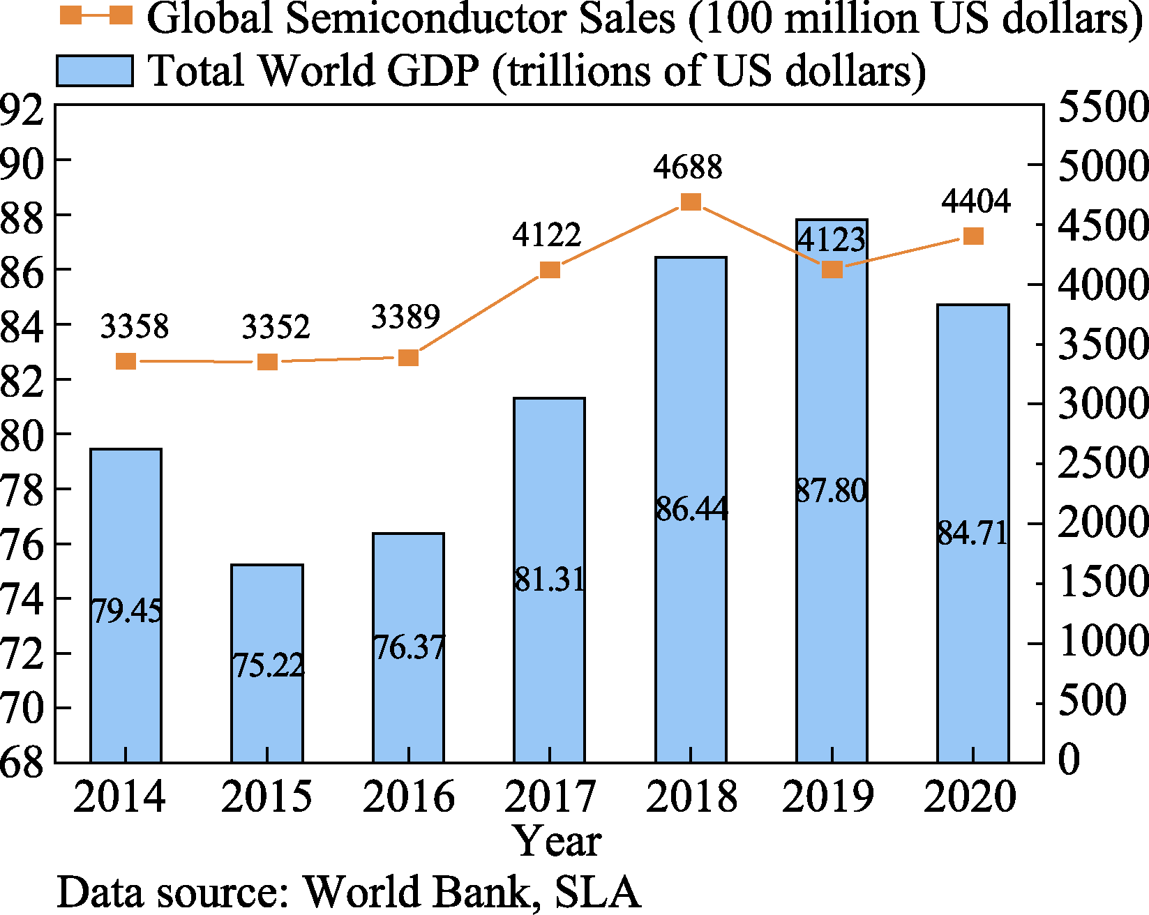
图1 2014-2020年全球GDP总额和半导体市场规模[7]
Fig. 1 Global GDP and semiconductor market size in 2014-2020[7]
| Parameter | Si | GaAs | SiC | GaN | Diamond |
|---|---|---|---|---|---|
| Band gap/eV | 1.12 | 1.43 | 3.26 | 3.45 | 5.45 |
| Dielectric constant | 11.9 | 13.1 | 10.1 | 9 | 5.5 |
| Breakdown field/ (kV·cm-1) | 300 | 400 | 2200 | 2000 | 10000 |
| Electron mobility/(cm2·V-1·s-1) | 1500 | 8500 | 1000 | 1250 | 2200 |
| Hole mobility/ (cm2·V-1·s-1) | 600 | 400 | 115 | 850 | 850 |
| Thermal conductivity/ (W·cm-1·K-1) | 1.5 | 0.46 | 4.9 | 1.3 | 22 |
| Electron saturation drift velocity/(×107, cm·s-1) | 1 | 1 | 2 | 2.2 | 2.7 |
表1 主要半导体材料性能参数对比[10]
Table 1 Comparison on performance parameters of the main semiconductor material [10]
| Parameter | Si | GaAs | SiC | GaN | Diamond |
|---|---|---|---|---|---|
| Band gap/eV | 1.12 | 1.43 | 3.26 | 3.45 | 5.45 |
| Dielectric constant | 11.9 | 13.1 | 10.1 | 9 | 5.5 |
| Breakdown field/ (kV·cm-1) | 300 | 400 | 2200 | 2000 | 10000 |
| Electron mobility/(cm2·V-1·s-1) | 1500 | 8500 | 1000 | 1250 | 2200 |
| Hole mobility/ (cm2·V-1·s-1) | 600 | 400 | 115 | 850 | 850 |
| Thermal conductivity/ (W·cm-1·K-1) | 1.5 | 0.46 | 4.9 | 1.3 | 22 |
| Electron saturation drift velocity/(×107, cm·s-1) | 1 | 1 | 2 | 2.2 | 2.7 |
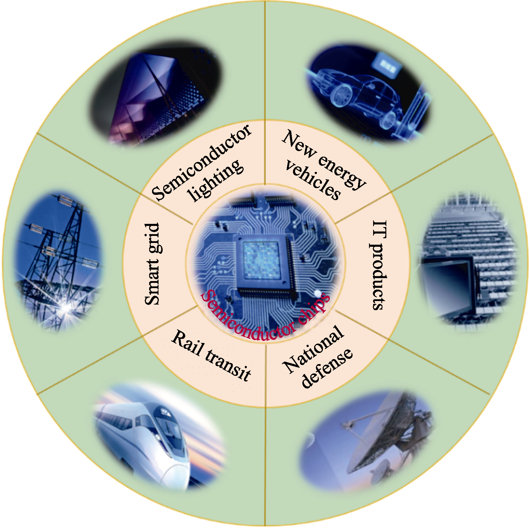
图2 第三代半导体应用领域
Fig. 2 Third-generation semiconductor applications
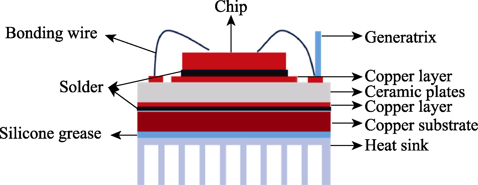
图3 典型功率半导体模块封装互连结构[14]
Fig. 3 Package interconnection structure of typical power semiconductor module[14]

图4 不同封装互连材料的使用温度范围和应用可能性[22]
Fig. 4 Applied temperature range and application possibilities of different package interconnect materials[22]
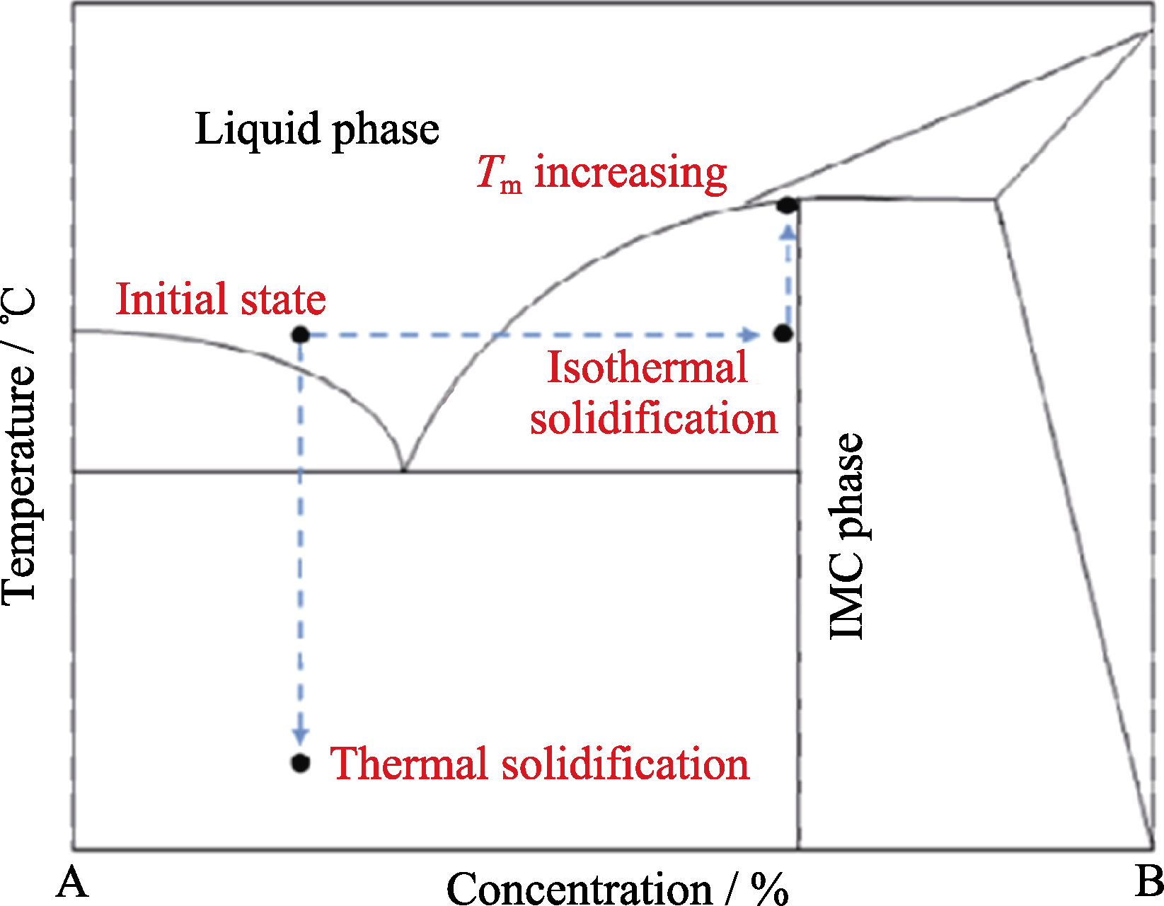
图5 TLP键合时的虚拟平衡相图[32]
Fig. 5 Virtual equilibrium phase diagram for TLP bonding[32]
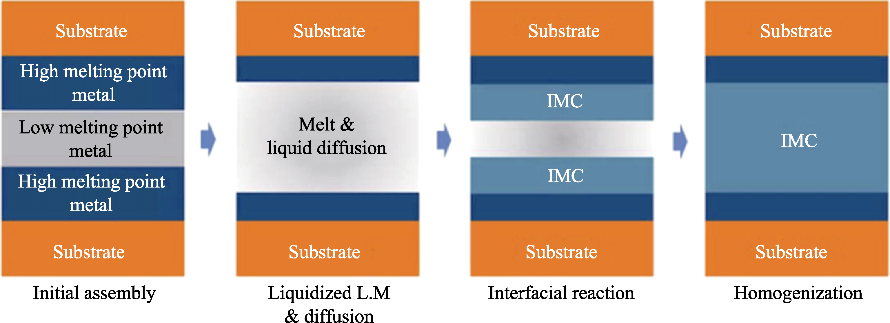
图6 TLP键合原理示意图[33]
Fig. 6 Schematic diagram of TLP bonding principle[33]
| Material | Temperature/℃ | Relative market price* | Relative performance | ||
|---|---|---|---|---|---|
| Bonding | IMC | Thermal conductivity | Electrical conductivity | ||
| Cu-Sn | 280 | 415(Cu6Sn5) | Cu: 0.5 | Cu: 4.4 | Cu: 4.1 |
| 676(Cu3Sn) | Sn: 0.8 | ||||
| Ni-Sn | 300 | 800(Ni3Sn3) | Ni: 1 | Ni: 1 | Ni: 1 |
| Sn: 0.8 | |||||
| Au-Sn | 250 | 419(AuSn) | Au: 2600 | Au: 3.5 | Au: 3.1 |
| Sn: 0.8 | |||||
| Ag-Sn | 250 | 480(Ag3Sn) | Ag: 63 | Ag: 4.7 | Ag: 4.4 |
| Sn: 0.8 | |||||
| Ag-In | 200 | 495 | Ag: 63 | Ag: 4.7 | Ag: 4.7 |
| In: 37.5 | |||||
| Au-In | 175 | 880 | Au: 2600 | Au: 3.1 | Au: 3.1 |
| In: 37.5 | |||||
表2 各种TLP键合材料及其性能[60]
Table 2 Various TLP bonding materials and their properties[60]
| Material | Temperature/℃ | Relative market price* | Relative performance | ||
|---|---|---|---|---|---|
| Bonding | IMC | Thermal conductivity | Electrical conductivity | ||
| Cu-Sn | 280 | 415(Cu6Sn5) | Cu: 0.5 | Cu: 4.4 | Cu: 4.1 |
| 676(Cu3Sn) | Sn: 0.8 | ||||
| Ni-Sn | 300 | 800(Ni3Sn3) | Ni: 1 | Ni: 1 | Ni: 1 |
| Sn: 0.8 | |||||
| Au-Sn | 250 | 419(AuSn) | Au: 2600 | Au: 3.5 | Au: 3.1 |
| Sn: 0.8 | |||||
| Ag-Sn | 250 | 480(Ag3Sn) | Ag: 63 | Ag: 4.7 | Ag: 4.4 |
| Sn: 0.8 | |||||
| Ag-In | 200 | 495 | Ag: 63 | Ag: 4.7 | Ag: 4.7 |
| In: 37.5 | |||||
| Au-In | 175 | 880 | Au: 2600 | Au: 3.1 | Au: 3.1 |
| In: 37.5 | |||||
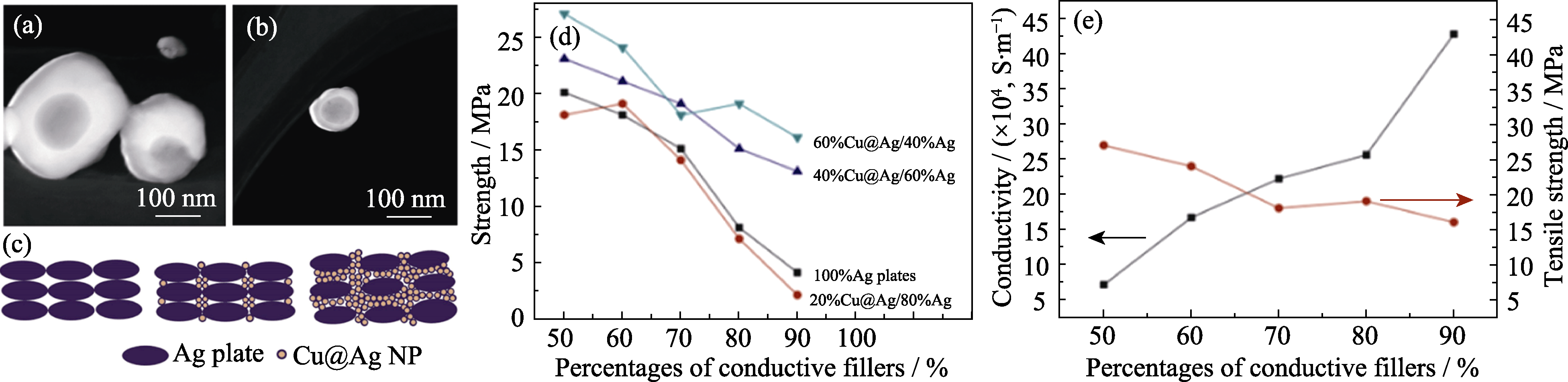
图7 Cu@Ag纳米颗粒及性能表征[85]
Fig. 7 Cu@Ag nanoparticles and performance characterization[85] (a, b) STEM images of Cu@Ag nanoparticles; (c) Schematic diagram of the filling effect of nanoparticles on silver conductive adhesive; (d) Influence of the conductive fillers’ percentages on the strength of the conductive adhesives; (e) Dependence of conductive fillers’ percentages on the strength and conductivity of conductive adhesive with 60%Cu@Ag/40% Ag plates
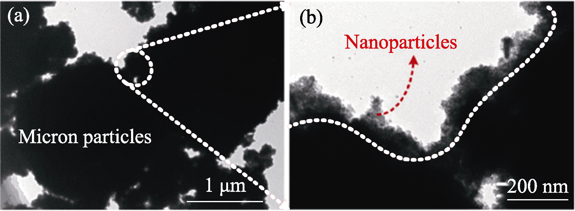
图8 不同粒径混合的微纳米铜颗粒结构[90]
Fig. 8 Structures of micro-nano copper particles mixed with different particle sizes[90] (a) TEM image showing micron particles; (b) TEM image showing nanoparticles
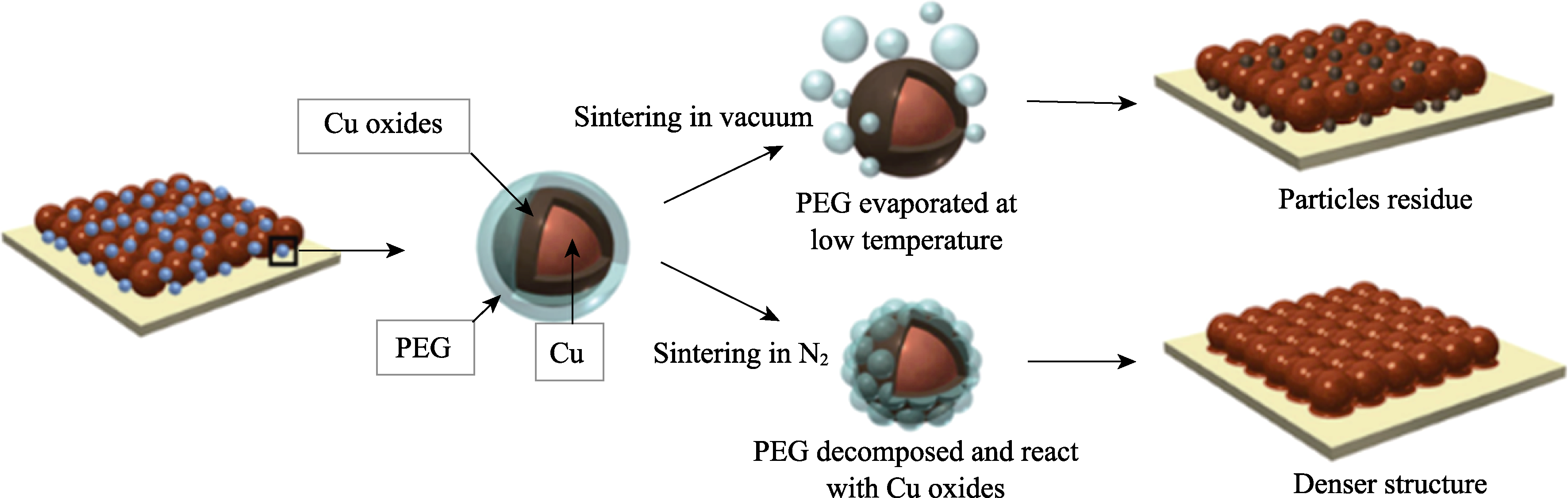
图9 双峰铜浆在不同气氛下的烧结示意图[93]
Fig. 9 Schematic diagram of sintering of bimodal copper slurry under different atmospheres[93]
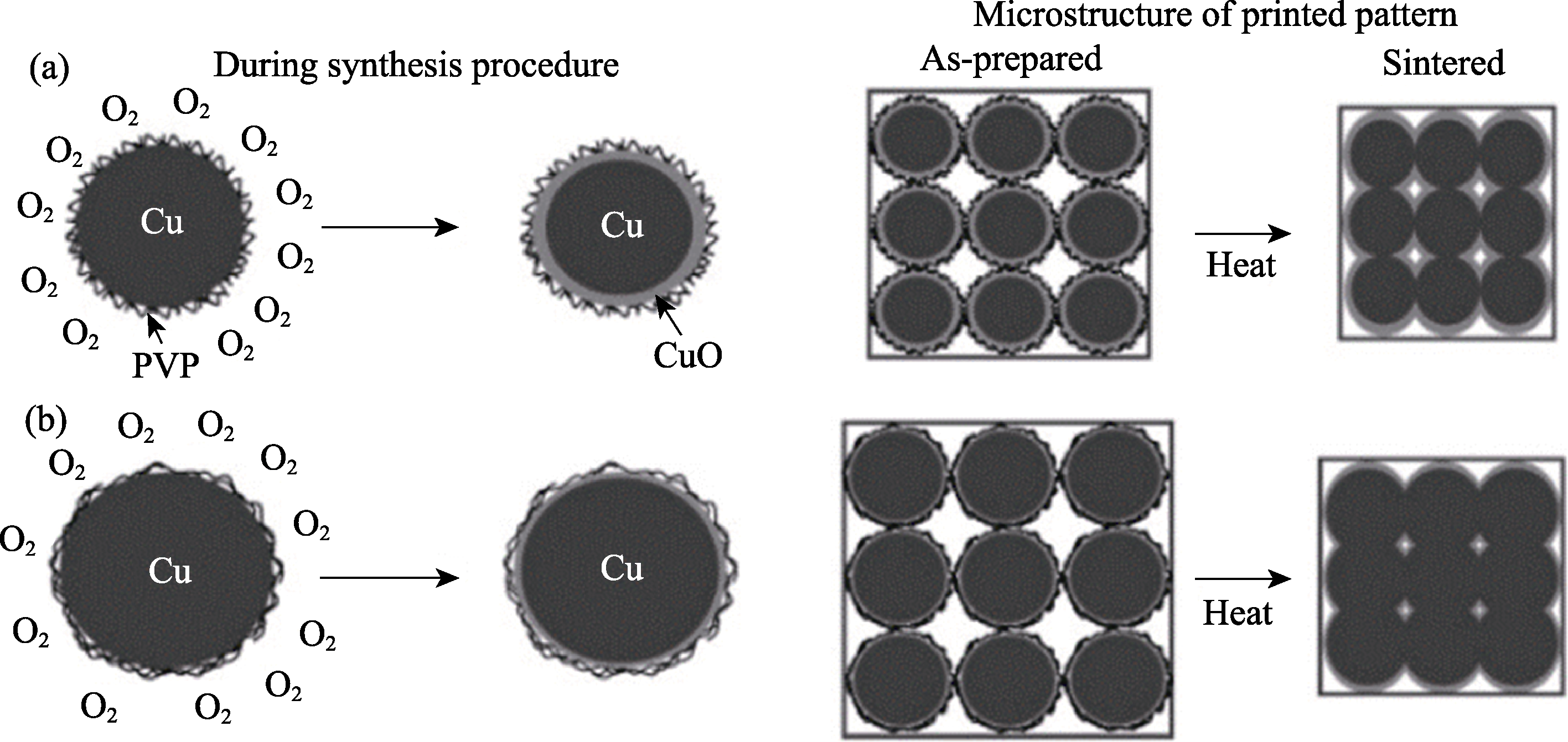
图10 铜纳米颗粒表层氧化对烧结性能的影响示意图[94]
Fig. 10 Schematic diagram of oxidation effect of surface layer of copper nanoparticles on the sintering performance[94] (a) With CuO outer layer; (b) No CuO outer layer
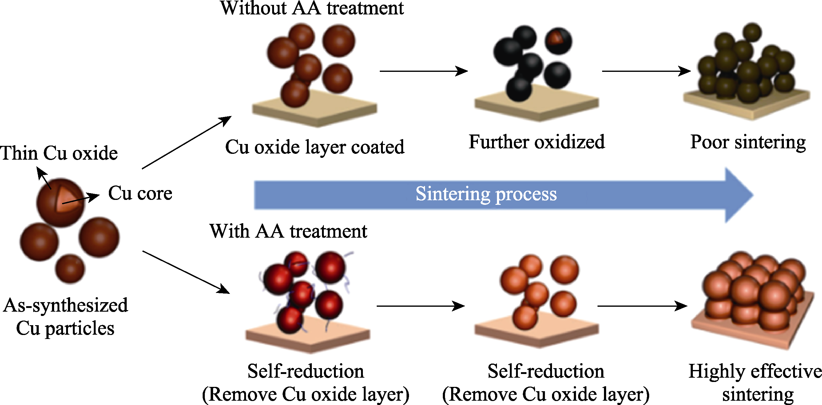
图11 抗坏血酸(AA)在铜浆中的促进作用机理[96]
Fig. 11 Mechanism of promotion in copper slurry by ascorbic acid (AA)[96]
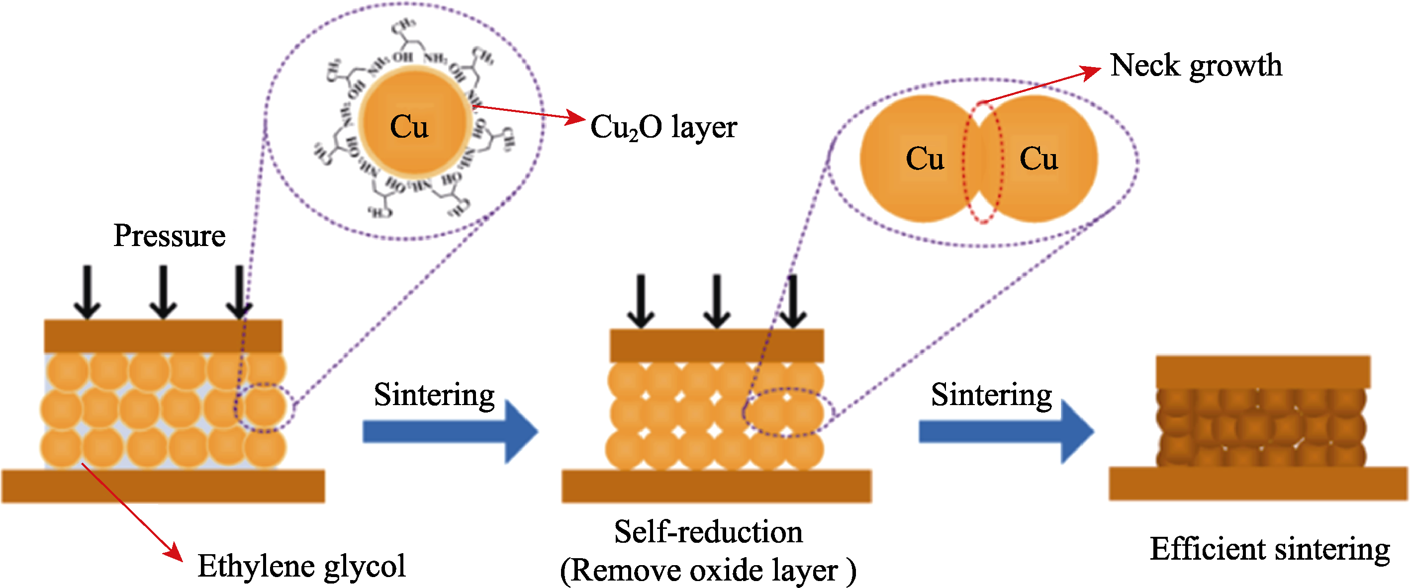
图12 Cu NP膏体还原和烧结机理示意图[98]
Fig. 12 Schematic diagram of reduction and sintering mechanism of Cu NP paste[98]
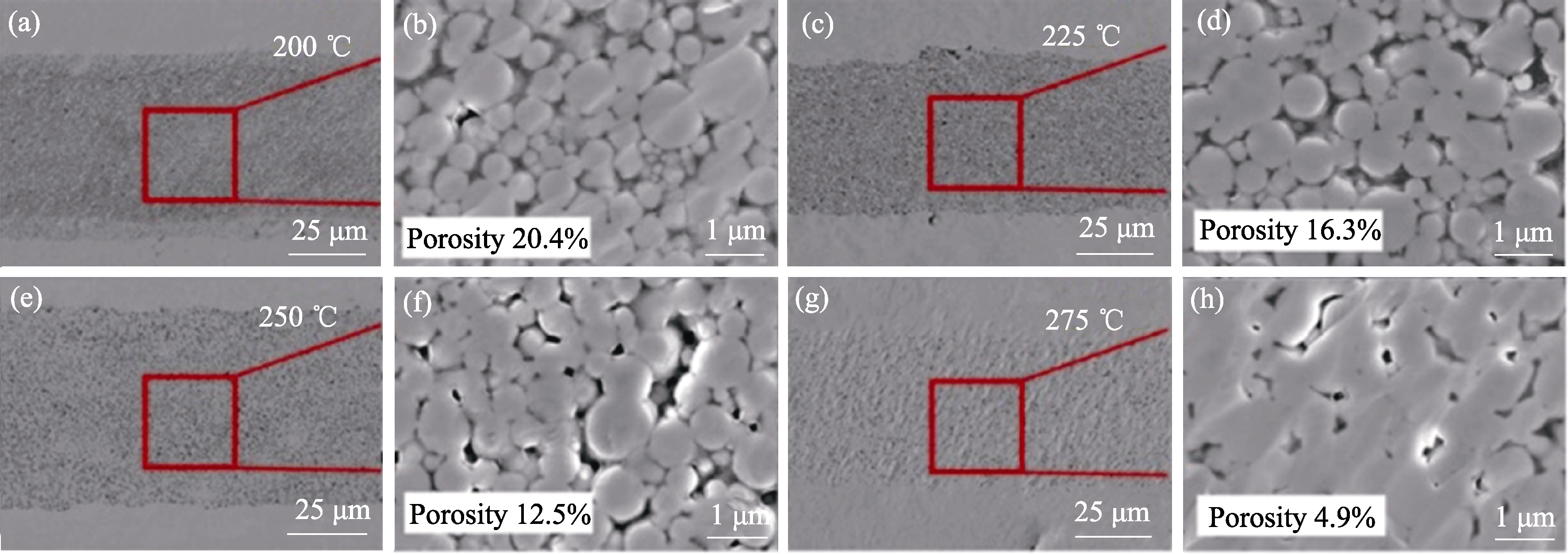
图13 在不同温度下烧结试样的截面SEM照片[102]
Fig. 13 SEM images of cross sections of sintered specimens at different temperatures[102] (a, b) 200 ℃; (c, d) 225 ℃; (e, f) 250 ℃; (g, h) 275 ℃
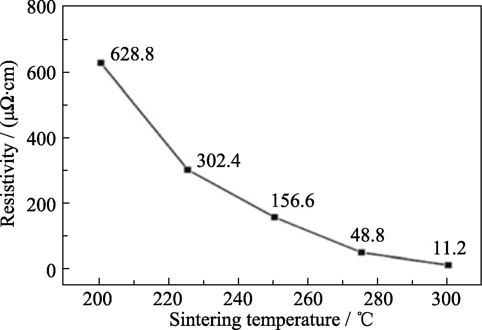
图14 结合层在不同烧结温度下的电阻率[103]
Fig. 14 Resistivities of the bonding layer at different sintering temperatures[103]
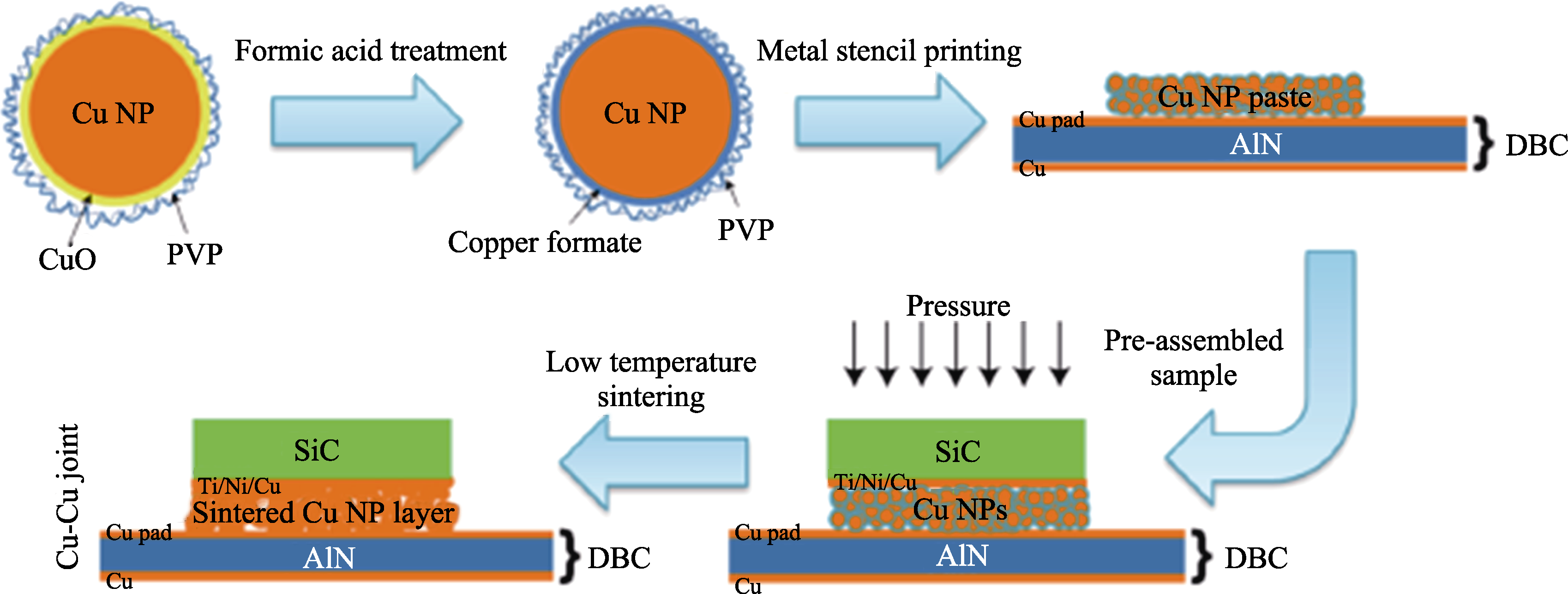
图15 Cu-Cu连接接头的制备过程示意图[104]
Fig. 15 Schematic diagram of the preparation process of Cu-Cu connection joints[104]
| Particle size | Appearance | Sintering process | Electrical conductivity/ (μΩ·cm) | Shearing performance/ MPa | Ref. |
|---|---|---|---|---|---|
| 10 and 1000 nm particle compound | Irregular | Ar, 250 ℃, 2 MPa, 15 min | 5.44 | 45.6 | [ |
| 200 nm, 1000 nm | Spherical | N2, 350 ℃, 0.4 MPa | - | 40 | [ |
| 530 nm | Irregular | 97% N2-3% H2, 300 ℃, 30 min | - | 23 | [ |
| 60-100 nm | Angular | N2, 200 ℃, 60 min | 18 | - | [ |
| Thick 200 nm, length 3-5 μm | Spherical | N2, 275 ℃, 10 MPa, 30 min | - | 50 | [ |
| 30-400 nm | Angular | N2, 300 ℃, 0.4 MPa, 30 min | - | 24.8 | [ |
| 6.5 nm | Spherical | Ar, 250 ℃, 5 MPa, 30 min | - | 36.2 | [ |
| 100 nm | Spherical | Air, 225 ℃, 8 MPa, 10 min | 59±7 | 28.7±1.6 | [ |
| 500 nm | Angular | HCOOH, 275 ℃, 5 MPa, 30 min | - | 70 | [ |
| 60.5 nm | Spherical | 95% Ar-5% H2, 300 ℃, 1.08 MPa, 60 min | 11.2 | 31.88 | [ |
| 30 nm | Spherical | 95% N2-5% H2, 320 ℃, 10 MPa, 5 min | 3.16 | 51.7 | [ |
| 54-64 nm | Sphere-like | H2, 400 ℃, 1.2 MPa, 5 min | - | 37.7 | [ |
| 5 nm | Sphere-like | 95% Ar-5% H2, 250 ℃, 1.08 MPa, 60 min | 4.1 | 25.36 | [ |
| 400-1200 nm | Sphere-like | Air, 200 ℃, 50 s | 54±2 | - | [ |
| 300-400 nm | Sphere-like | N2, 200 ℃, 30 min | 139±24 | - | [ |
| 1-3 μm | Sphere-like | Air, 180 ℃, 5 min | 30 | - | [ |
| 200 nm | Spherical | Air, 300 ℃, 2 MPa, 1 min | - | 21.8 | [ |
| 50 nm | Spherical | Air, 220 ℃, 5 min | - | 30 | [ |
| 10 nm | Spherical | N2, 200 ℃, 30 min | 14.0±4.5 | - | [ |
| 6.5 nm | Spherical | Air, 175 ℃, 2 MPa, 10 min | - | 35.1 | [ |
| 60 nm | Sphere-like | 95% Ar-5% H2, 250 ℃, 10 MPa, 60 min | - | 32.4 | [ |
| 4.4 nm | Angular | N2, 150 ℃, 30 min | 52 | - | [ |
| Tens to hundreds of nanometers | Irregular | Vacuum, 300 ℃, 0.4 MPa,30 min | - | 20 | [ |
| <10 nm | Angular | Ar, 250 ℃, 3 MPa, 30 min | 5.1 | - | [ |
表3 各种低温烧结工艺及性能对比
Table 3 Comparison of various low-temperature sintering processes and their performance
| Particle size | Appearance | Sintering process | Electrical conductivity/ (μΩ·cm) | Shearing performance/ MPa | Ref. |
|---|---|---|---|---|---|
| 10 and 1000 nm particle compound | Irregular | Ar, 250 ℃, 2 MPa, 15 min | 5.44 | 45.6 | [ |
| 200 nm, 1000 nm | Spherical | N2, 350 ℃, 0.4 MPa | - | 40 | [ |
| 530 nm | Irregular | 97% N2-3% H2, 300 ℃, 30 min | - | 23 | [ |
| 60-100 nm | Angular | N2, 200 ℃, 60 min | 18 | - | [ |
| Thick 200 nm, length 3-5 μm | Spherical | N2, 275 ℃, 10 MPa, 30 min | - | 50 | [ |
| 30-400 nm | Angular | N2, 300 ℃, 0.4 MPa, 30 min | - | 24.8 | [ |
| 6.5 nm | Spherical | Ar, 250 ℃, 5 MPa, 30 min | - | 36.2 | [ |
| 100 nm | Spherical | Air, 225 ℃, 8 MPa, 10 min | 59±7 | 28.7±1.6 | [ |
| 500 nm | Angular | HCOOH, 275 ℃, 5 MPa, 30 min | - | 70 | [ |
| 60.5 nm | Spherical | 95% Ar-5% H2, 300 ℃, 1.08 MPa, 60 min | 11.2 | 31.88 | [ |
| 30 nm | Spherical | 95% N2-5% H2, 320 ℃, 10 MPa, 5 min | 3.16 | 51.7 | [ |
| 54-64 nm | Sphere-like | H2, 400 ℃, 1.2 MPa, 5 min | - | 37.7 | [ |
| 5 nm | Sphere-like | 95% Ar-5% H2, 250 ℃, 1.08 MPa, 60 min | 4.1 | 25.36 | [ |
| 400-1200 nm | Sphere-like | Air, 200 ℃, 50 s | 54±2 | - | [ |
| 300-400 nm | Sphere-like | N2, 200 ℃, 30 min | 139±24 | - | [ |
| 1-3 μm | Sphere-like | Air, 180 ℃, 5 min | 30 | - | [ |
| 200 nm | Spherical | Air, 300 ℃, 2 MPa, 1 min | - | 21.8 | [ |
| 50 nm | Spherical | Air, 220 ℃, 5 min | - | 30 | [ |
| 10 nm | Spherical | N2, 200 ℃, 30 min | 14.0±4.5 | - | [ |
| 6.5 nm | Spherical | Air, 175 ℃, 2 MPa, 10 min | - | 35.1 | [ |
| 60 nm | Sphere-like | 95% Ar-5% H2, 250 ℃, 10 MPa, 60 min | - | 32.4 | [ |
| 4.4 nm | Angular | N2, 150 ℃, 30 min | 52 | - | [ |
| Tens to hundreds of nanometers | Irregular | Vacuum, 300 ℃, 0.4 MPa,30 min | - | 20 | [ |
| <10 nm | Angular | Ar, 250 ℃, 3 MPa, 30 min | 5.1 | - | [ |
| [1] |
TSUYOSHI F, JUAN C B, JEREMY J, et al. Power conversion with SiC devices at extremely high ambient temperature. IEEE Transactions on Power Electronics, 2007, 22(4):1321.
DOI URL |
| [2] |
TSUYOSHI F, HIROYASU I, MASASHI S, et al. Characterization of SiC power module for high switching frequency operation. IEICE Electronics Express, 2010, 7(14):1008.
DOI URL |
| [3] | JOHNSON R W, PALMER M, WANG C, et al. Packaging materials and approaches for high temperature SiC power devices. Advancing Microelectronics, 2004, 31(1):8. |
| [4] |
MCCLUSKEY F P, DASH M, WANG Z, et al. Reliability of high temperature solder alternatives. Microelectronics Reliability, 2006, 46(9/10/11): 1910.
DOI URL |
| [5] | 中华人民共和国科学技术部. “十三五”材料领域科技创新专项规划(2017), 306082017496. 北京: 中华人民共和国科学技术部, 2017: 1-29. |
| [6] | XIE M, GAN Y, WANG H. Research on the strategy of new material power for 2035. Strategic Study of CAE, 2020, 22(5):1. |
| [7] | MA Y, TU X J. Global IC industry: growth, migration and remodeling. Information and Communications Technology and Policy, 2022, 48(5):68. |
| [8] | HUANG F L, ZHU H. Semiconductor integrated circuit business unit management strategy. Manager Journal, 2020, 8: 58. |
| [9] | WANG X. Application status and development trend of semiconductor materials. Lamps & Lighting, 2022, 1: 67. |
| [10] | CAO J, ZHANG Z Q. Advances in silicon carbide power module packaging technology. Applications of IC, 2018, 35(8):20. |
| [11] | WANG R D. Advanced packaging promotes new development of semiconductor industry. China Integrated Circuit, 2022, 31(4):26. |
| [12] | WU Y B, DAI X P, WANG Y G, et al. Research progress on advanced interconnect technologies in IGBT power module packaging. High Power Converter Technology, 2015 (2): 6. |
| [13] | YUAN G Z. Micro-scale mechanical properties of lead-free solder joint interconnect interfaces for electronic packaging. Taiyuan: Master's Thesis, Taiyuan University of Technology, 2016. |
| [14] | XU H Y, XU H Y, ZANG L K, et al. Advances in low-temperature sintered copper-based electronic pastes for power device chip interconnects. Electronic Components & Materials, 2022, 41(1):9. |
| [15] | DONG Z Z. Research on some key issues of low-power silicon carbide integrated modules. Hangzhou: Master's Thesis, Zhejiang University, 2022. |
| [16] | HARTNETT A, BUERKI S.Process and reliability advantages of AuSn eutectic die-attach. IMAPS 2009 International Symposium on Microelectronics. San Jose, CA(US), 2009: 470-474. |
| [17] | HUMSTON G, JACOBSON D. Principles of soldering and brazing. Materials Park, OH, USA: ASM International, 1993. |
| [18] | FAN J L. Controlled preparation and low-temperature sintering of silver/copper nanoparticles and their interconnection applications in microelectronic packaging. Shenzhen: Doctoral dissertation, University of Chinese Academy of Sciences (Shenzhen Institutes of Advanced Technology, Chinese Academy of Sciences), 2020. |
| [19] | SHEN B W, LIU G H, GAO L Q, et al. Research progress of new low temperature lead-free solder. Precious Metals, 2022, 43(S1):1. |
| [20] | GANESAN SANKA, PECHT MICHAEL. Lead-free electronics. Hoboken N.J.: Wiley-Interscience, 2006. |
| [21] |
ZHANG H W, MINTER J, LEE N C. A brief review on high- temperature, Pb-free die-attach materials. Journal of Electronic Materials, 2019, 48(1):201.
DOI |
| [22] |
MANIKAM V R, CHEONG K Y. Die attach materials for high temperature applications: a review. IEEE Transactions on Components Packaging and Manufacturing Technology, 2011, 1(4):457.
DOI URL |
| [23] | VIVEK C, JESPER H, JOHN H. Design of lead-free candidate alloys for high-temperature soldering based on the Au-Sn system. Materials and Design, 2010, 31: 4638. |
| [24] | HARPSTER T J, NAJAFI K. Field-assisted bonding of glass to Si-Au eutectic solder for packaging applications. 16th IEEE Annual International Conference on Micro Electro Mechanical Systems. Kyoto, Japan: IEEE, 2003. |
| [25] | DREVIN B A, BADAWI F, LACROIX F, et al. Investigation of die attach for SiC power device for 300 ℃ applications. 9th European Conference on Silicon Carbide and Related Materials (ECSCRM 2012). Saint Petersburg, Russia: Trans Tech Publications Ltd, 2012. |
| [26] | HASSAM S, ROGEZ J, BAHARI Z. Experimental phase diagram of the AuSb-InSb section in the Au-In-Sb system. Journal of Chemical Thermodynamics, 2014, 70: 168. |
| [27] |
HUANG M L, HUANG F F, YANG Y C. Composition design of Sn-rich Sn-Au-Ag solders using cluster-plus-glue-atom model. Journal of Materials Science: Materials in Electronics, 2017, 28(15):11192.
DOI URL |
| [28] | LAU B L, HAN Y, ZHANG H Y, et al. Development of fluxles bonding using deposited gold-indium multi-layer composite for heterogeneous silicon micro-cooler stacking. IEEE 16th Electronics Packaging Technology Conference (EPTC). Marina Bay Sands, Singapore: IEEE, 2014. |
| [29] | KOSTOV A, GOMIDZELOVIC L, MILOSAVLJEVIC A, et al. Thermodynamic characterization of solder Au-Ga alloys. Materials Chemistry and Physics, 2020, 241: 122278. |
| [30] | XU J C, WU M F, PU J, et al. Novel Au-based solder alloys: a potential answer for electrical packaging problem. Advances in Materials Science and Engineering, 2020, 2020: 4969647. |
| [31] |
LEONARD B. Semiconductor joining by the solid-liquid-interdiffusion (SLID) proces. Journal of The Electrochemical Society, 1966, 113(12):1282.
DOI URL |
| [32] |
JUNG D H, SHARMAL A, MAYER M, et al. A review on recent advances in transient liquid phase (TLP) bonding for thermoelectric power module. Reviews on Advanced Materials Science, 2018, 53(2):147.
DOI URL |
| [33] | ROH M H, NISHIKAWA H, JUNG J P, et al. Trasient liquid phase bonding for power semiconductor. The Korean Microelectronics and Packaging Society, 2017, 24(1):27. |
| [34] |
MITTAL J, LIN K L. Diffusion of Cu and interfacial reactions during reflow of Sn-8.5Zn-0.5Ag-0.01Al-0.1Ga alloy on Ni/Cu substrate. Journal of Materials Research, 2012, 27(8):1142.
DOI URL |
| [35] |
YU C C, SU P C, BAI S J, et al. Nickel-tin solid-liquid inter- diffusion bonding. International Journal of Precision Engineering and Manufacturing, 2014, 15(1):143.
DOI URL |
| [36] |
HSU H H, HUANG Y T, HUANG S Y, et al. Evolution of the intermetallic compounds in Ni/Sn-2.5Ag/Ni microbumps for three-dimensional integrated circuits. Journal of Electronic Materials, 2015, 44(10):3888.
DOI URL |
| [37] |
SHIH W L, YANG T L, CHUANG H Y, et al. Inhibition of gold embrittlement in micro-joints for three-dimensional integrated circuits. Journal of Electronic Materials, 2014, 43(11):4262.
DOI URL |
| [38] |
CAO Y H, NING W G, LUO L. Wafer-level package with simultaneous TSV connection and cavity hermetic sealing by solder bonding for MEMS device. IEEE Transactions on Electronics Packaging Manufacturing, 2009, 32(3):125.
DOI URL |
| [39] |
HANG C J, TIAN Y H, ZHANG R, et al. Phase transformation and grain orientation of Cu-Sn intermetallic compounds during low temperature bonding process. Journal of Materials Science: Materials in Electronics, 2013, 24(10):3905.
DOI URL |
| [40] | YANG T L, AOKI T, MATSUMOTO K, et al. Full intermetallic joints for chip stacking by using thermal gradient bonding. Acta Materialia, 2016, 113: 90. |
| [41] | FENG J Y, HANG C J, TIAN Y H, et al. Growth kinetics of Cu6Sn5 intermetallic compound in Cu-liquid Sn interfacial reaction enhanced by electric current. Scientific Reports, 2018, 8: 1175. |
| [42] | LIU B L, TIAN Y H, WANG C X, et al. Ultrafast formation of unidirectional and reliable Cu3Sn-based intermetallic joints assisted by electric current. Intermetallics, 2017, 80: 26. |
| [43] | ZHAO H Y, LIU J H, LI Z L, et al. Non-interfacial growth of Cu3Sn in Cu/Sn/Cu joints during ultrasonic-assisted transient liquid phase soldering process. Materials Letters, 2017, 186: 283. |
| [44] |
ZHAO H Y, LIU J H, LI Z L, et al. A comparative study on the microstructure and mechanical properties of Cu6Sn5 and Cu3Sn joints formed by TLP soldering with/without the assistance of ultrasonic waves. Metallurgical and Materials Transactions A, 2018, 49(7):2739.
DOI |
| [45] |
CAIN S R, WILCOX J R, VENKATRAMAN R. A diffusional model for transient liquid phase bonding. Acta Materialia, 1997, 45(2):701.
DOI URL |
| [46] |
MARAUSKA S, CLAUS M, LISEC T, et al. Low temperature transient liquid phase bonding of Au/Sn and Cu/Sn electroplated material systems for MEMS wafer-level packaging. Microsystem Technologies, 2013, 19(8):1119.
DOI URL |
| [47] |
BOBZIN K, BAGCIVAN N, ZHAO L D, et al. Development of new transient liquid phase system Au-Sn-Au for microsystem technology. Frontiers of Mechanical Engineering in China, 2010, 5(4):370.
DOI URL |
| [48] |
TOLLEFSEN T A, LARSSON A, TAKLO M M V, et al. Au-Sn SLID bonding: a reliable HT interconnect and die attach technology. Metallurgical and Materials Transactions B, 2013, 44(2):406.
DOI URL |
| [49] |
RAUTIAINEN A, XU H, OSTERLUND E, et al. Microstructural characterization and mechanical performance of wafer-level SLID bonded Au-Sn and Cu-Sn seal rings for MEMS encapsulation. Journal of Electronic Materials, 2015, 44(11):4533.
DOI URL |
| [50] |
LIN W P, LEE C C. Fluxless bonding of bismuth telluride chips to Alumina using Ag-In system for high temperature thermoelectric devices. IEEE Transactions on Components, Packaging, and Manufacturing Technology, 2011, 1(9):1311.
DOI URL |
| [51] |
LI J F, AGYAKWA P A, JOHNSON C M. Kinetics of Ag3Sn growth in Ag-Sn-Ag system during transient liquid phase soldering process. Acta Materialia, 2010, 58(9):3429.
DOI URL |
| [52] |
GOLLAS B, ALBERING J H, SCHMUT K, et al. Thin layer in situ XRD of electrodeposited Ag/Sn and Ag/In for low temperature isothermal diffusion soldering. Intermetallics, 2008, 16(8):962.
DOI URL |
| [53] |
LIS A, LEINENBACH C. Effect of process and service conditions on TLP-bonded components with (Ag,Ni-)Sn interlayer combinations. Journal of Electronic Materials, 2015, 44(11):4576.
DOI URL |
| [54] | SHAO H K, WU A P, BAO Y D, et al. Microstructure characterization and mechanical behavior for Ag3Sn joint produced by foil- based TLP bonding in air atmosphere. Materials Science & Engineering A, 2017, 680: 221. |
| [55] |
ZHANG W, RUYTHOOREN W. Study of the Au/In reaction for transnsient liquid-phase bonding and 3D chip stackaging. Journal of Electronic Materials, 2008, 37(8):1095.
DOI URL |
| [56] | YOON J W, LEE B S. Initial interfacial reactions of Ag/In/Ag and Au/In/Au joints during transient liquid phase bonding. Microelectronic Engineering, 2018, 201: 6. |
| [57] | CHOI W K, PREMACHANDRAN C S, CHIEW O S, et al. Development of novel intermetallic joints using thin film indium-based solder by low temperature bonding technology for 3D IC stacking. 2009 IEEE 59th Electronic Components and Technology Conference, San Diego, CA, USA, 2009: 333-338. |
| [58] |
LIN J C, HUANG L W, JANG G Y, et al. Solid-liquid interdiffusion bonding between In-coated silver thick films. Thin Solid Films, 2002, 410 (1/2): 212.
DOI URL |
| [59] | LEE C K, YU A B, YAN L L, et al. Characterization of intermediate In/Ag layers of low temperature fluxless solder based wafer bonding for MEMS packaging. Sensors and Actuators A: Physical, 2009, 154: 85. |
| [60] | MOKHTARI O. A review: formation of voids in solder joint during the transient liquid phase bonding process-causes and solutions. Microelectronics Reliability, 2019, 98: 95. |
| [61] | ZHANG W, YAO J J, ZHAN K, et al. Conductive adhesive research progress. Science & Technology Review, 2018, 36(10):56. |
| [62] | LI Y, LU D, WONG C P.Electrical conductive adhesives with nanotechnologies. New York: Springer New York, NY, 2010. |
| [63] | LI S H. Gold conductive adhesive. China Adhesives, 1998(6): 33. |
| [64] | WANG Y H, HUANG A, XIE H, et al. Isotropical conductive adhesives with very-long silver nanowires as conductive fillers. Journal of Materials Science: Materials Electronics, 2017, 28: 10. |
| [65] | XIONG S H, YANG R C, WU D, et al. The effect of silver powder morphology and size on the performance of conductive adhesives. Electronic Components & Materials, 2005, 24(8):14. |
| [66] | WAN C, WANG H Q, DU B, et al. The effect of silver powder morphology and surface treatment on the performance of conductive adhesives. Electronics Process Technology, 2011, 32(2):72. |
| [67] | QIAO W Y, BAO H, LI X H, et al. Research on electrical conductive adhesives filled with mixed filler. International Journal of Adhesion and Adhesives, 2014, 48: 159. |
| [68] | WU H P, WU X J, GE M Y, et al. Effect analysis of filler sizes on percolation threshold of isotropical conductive adhesives. Composites Science and Technology, 2007, 67: 1116. |
| [69] | YIM M J, LI Y, MOON K S, et al. Oxidation prevention and electrical property enhancement of copper-filled isotropically conductive adhesives. Journal of Electronic Materials, 2007, 36(10):1342. |
| [70] | LIU Y X, WANG X D, GU Y X, et al. Development of copper powder-added conductive adhesive. China Adhesives, 2008, 17(11):27. |
| [71] | PENG Y H, YANG C H, CHEN K T, et al. Study on synthesis of ultrafine Cu-Ag core-shell powders with high electrical conductivity. Applied Surface Science, 2012, 263: 38. |
| [72] |
HO L N, NISHIKAWA H, TAKEMOTO T. Effect of different copper fillers on the electrical resistivity of conductive adhesives. Journal of Materials Science Materials in Electronics, 2011, 22(5):538.
DOI URL |
| [73] | FAN Y Q, GU Y W, XIA X Y. Preparation and properties of fibrous copper powder conductive filler. Electronic Components & Materials, 2014, 33(8):25. |
| [74] | WANG J H, MIN H L. Research on nickel powder conductive acrylate pressure sensitive adhesive. Insulating Materials, 2006(5): 4. |
| [75] |
PU N W, PENG Y Y, WANG P C, et al. Application of nitrogen- doped graphene nanosheets in electrically conductive adhesives. Carbon, 2014, 67(2):449.
DOI URL |
| [76] |
MARCQ F, DEMONT P, MONFRAIX P, et al. Carbon nanotubes and silver flakes filled epoxy resin for new hybrid conductive adhesives. Microelectronics Reliability, 2011, 51(7):1230.
DOI URL |
| [77] |
YIM B S, KIM J M. Characteristics of isotropically conductive adhesive (ICA) filled with carbon nanotubes (CNTs) and low-melting-point alloy fillers. Materials Transactions, 2010, 51(12):2329.
DOI URL |
| [78] | WU H P, WU X J, LIU J F, et al. Properties of carbon nanotube- filled isotropic conductive adhesives. Acta Materiae Compositae Sinica, 2006, 23(2):9. |
| [79] |
AMOLI B M, TRINIDAD J, HU A, et al. Highly electrically conductive adhesives using silver nanoparticle (Ag NP)-decorated graphene: the effect of NPs sintering on the electrical conductivity improvement. Journal of Materials Science Materials in Electronics, 2015, 26(1):590.
DOI URL |
| [80] | MA M Z, MA H R, ZENG J F, et al. In situ hydrothermal synthesis of graphene-based nanosilver and its application in conductive adhesives. Journal of Shihezi University (Natural Science), 2017, 35(1):12. |
| [81] | SU Y, DAI Y Q, LIAO B, et al. Research progress of conductive filler for conductive adhesive. China Adhesives, 2018, 27(10):52. |
| [82] |
BEHNAM M A, HU A M, ZHOU N Y, et al. Recent progresses on hybrid micro-nano filler systems for electrically conductive adhesives (ECAs) applications. Journal of Materials Science: Materials in Electronics, 2015, 26(7):4730.
DOI URL |
| [83] | ZHANG W F. Pressureless sintering of micrometer silver pastes for electrical connections and their properties. Fuzhou: Master's Thesis, Fujian Normal University, 2019. |
| [84] | ZUO X. Preparation and performance study of high thermal conductive adhesive. China Adhesives, 2022, 31(10):47. |
| [85] |
ZHANG J G, LIANG M H, HU Q, et al. Cu@Ag nanoparticles doped micron-sized Ag plates for conductive adhesive with enhanced conductivity. International Journal of Adhesion and Adhesives, 2020, 102(1):102657.
DOI URL |
| [86] | YANG J L, DONG C C, LUO J. Advances in low-temperature sintering of nanosilver in novel power module packages. Materials Reports, 2019, 33(S2):360. |
| [87] |
SCHWARZBAUER H, KUHNERT R. Novel large area joining technique for improved power device performance. IEEE Transactions on Industry Applications, 1991, 27(1):93.
DOI URL |
| [88] | HIROSHI N, TOMOAKJ H, TADASHI T. Effects of joining conditions on joint strength of Cu/Cu joint using Cu nanoparticle paste. The Open Surface Science Journal, 2011, 3: 60. |
| [89] | HERRING C. Diffusional viscosity of a polycrystalline solid. Journal of Applied Physics, 1950, 21(5):4375. |
| [90] |
PENG Y, MOU Y, LIU J X, et al. Fabrication of high-strength Cu-Cu joint by low-temperature sintering micron-nano Cu composite paste. Journal of Materials Science: Materials in Electronics, 2020, 31(11):8456.
DOI |
| [91] |
GAO Y, ZHANG H, LI W L, et al. Die bonding performance using bimodal Cu particle paste under different sintering atmospheres. Journal of Electronic Materials, 2017, 46(7):4575.
DOI URL |
| [92] |
MASTUDA T, YAMAGIWA D, FURUSAWA H, et al. Reduction behavior of surface oxide on submicron copper particles for pressureless sintering under reducing atmosphere. Journal of Electronic Materials, 2021, 51(1):1.
DOI |
| [93] |
LI Y, QI T K, CHEN M, et al. Mixed ink of copper nanoparticles and copper formate complex with low sintering temperatures. Journal of Materials Science: Materials in Electronics, 2016, 27(11):11432.
DOI URL |
| [94] |
JEONG S, WOO K, KIM D, et al. Controlling the thickness of the surface oxide layer on Cu nanoparticles for the fabrication of conductive structures by ink-jet printing. Advanced Functional Materials, 2008, 18(5):679.
DOI URL |
| [95] | BHOGARAJU S K, CONTI F, KOTADIA H R, et al. Novel approach to copper sintering using surface enhanced brass micro flakes for microelectronics packaging. Journal of Alloys and Compounds, 2020, 844: 156043. |
| [96] | GAO Y, LI W L, CHEN C T, et al. Novel copper particle paste with self-reduction and self-protection characteristics for die attachment of power semiconductor under a nitrogen atmosphere. Materials and Design, 2018, 160: 1265. |
| [97] |
MOU Y, LIU J X, CHENG H, et al. Facile preparation of self- reducible Cu nanoparticle paste for low temperature Cu-Cu bonding. JOM, 2019, 71(9):3076.
DOI |
| [98] |
WANG X C, ZHANG Z Q, FENG Y Y, et al. Anti-oxidative copper nanoparticle paste for Cu-Cu bonding at low temperature in air. Journal of Materials Science: Materials in Electronics, 2021, 33(2):817.
DOI |
| [99] |
JANG S, SEO Y, CHOI J, et al. Sintering of inkjet printed copper nanoparticles for flexible electronics. Scripta Materialia, 2010, 62(5):258.
DOI URL |
| [100] | XIANG D L, HIROSHI N. Improved joint strength with sintering bonding using microscale Cu particles by an oxidation-reduction process. IEEE 66th Electronic Components and Technology Conference, Las Vegas, USA, 2016: 455-460. |
| [101] |
YAMAKAWA T, TAKEMOTO T, SHIMODA M, et al. Influence of joining conditions on bonding strength of joints: efficacy of low-temperature bonding using Cu nanoparticle paste. Journal of Electronic Materials, 2013, 42(6):1260.
DOI URL |
| [102] |
LI J L, XU Y, ZHAO X L, et al. Enhancement and mechanism of copper nanoparticle sintering in activated formic acid atmosphere at low temperature. ECS Journal of Solid State Science and Technology, 2021, 10(5):054004.
DOI |
| [103] |
LI J J, YU X, SHI T L, et al. Low-temperature and low-pressure Cu-Cu bonding by highly sinterable Cu nanoparticle paste. Nanoscale Research Letters, 2017, 12(1):255.
DOI PMID |
| [104] | LIU J D, CHEN H T, JI H J, et al. Highly conductive Cu-Cu joint formation by low-temperature sintering of formic acid-treated Cu nanoparticles. ACS Applied Materials & Interfaces, 2016, 8(48):33289. |
| [105] | PA X, ZHOU J C, ZHANG J G, et al. Study on preparation and application of nano-copper powder for power semiconductor device packaging. China International Forum on Solid State Lighting & International Forum on Wide Bandgap Semiconductors China, Shenzhen, 2019: 54-58. |
| [106] | KOBAYASHI Y, SHIROCHI T, YASUDA Y, et al. A metal-metal bonding process using metallic copper nanoparticles prepared in aqueous solution. International Journal of Adhesion & Adhesives, 2014, 3(2):114. |
| [107] |
LI J J, LIANG Q H, FAN T L, et al. Design of Cu nanoaggregates composed of ultra-small Cu nanoparticles for Cu-Cu thermocompression bonding. Journal of Alloys and Compounds, 2019, 772(2019):793.
DOI URL |
| [108] |
QI T K, WANG X C, YANG J F, et al. Rapid low temperature sintering in air of copper submicron particles with synergistic surface-activation and anti-oxidative protection. Journal of Materials Science: Materials in Electronics, 2019, 30(13):12669.
DOI |
| [109] |
QI T K, ZHANG Z Q, LI Y, et al. A low temperature self- reducible copper hydroxide amino-alcohol complex catalyzed by formic acid for conductive copper films. Journal of Materials Chemistry C, 2018, 6(42):11320.
DOI URL |
| [110] |
AKIHIRO Y, YOHEI T, INDRA W F. Synthesis of copper conductive film by low-temperature thermal decomposition of coppereaminediol complexes under an air atmosphere. Materials Chemistry and Physics, 2014, 148(1/2):299.
DOI URL |
| [111] |
KIM M I, LEE J H. Die attachment by extremely fast pressure-assisted sintering of 200 nm Cu particles. Electronic Materials Letters, 2021, 17(3):286.
DOI |
| [112] | YANG Z, SADIE C S, MARK G, et al. High bond strength Cu joints fabricated by rapid and pressureless in situ reduction- sintering of Cu nanoparticles. Materials Letters, 2020, 276: 128260. |
| [113] |
DENG D Y, CHENG Y R, JIN Y X, et al. Antioxidative effect of lactic acid-stabilized copper nanoparticles prepared in aqueous solution. Journal of Materials Chemistry, 2012, 22(45):23989.
DOI URL |
| [114] | MOU Y, CHENG H, PENG Y, et al. Fabrication of reliable Cu-Cu joints by low temperature bonding isopropanol stabilized Cu nanoparticles in air. Materials Letters, 2018, 229: 353. |
| [115] | MOU Y, PENG Y, ZHANG Y, et al. Cu-Cu bonding enhancement at low temperature by using carboxylic acid surface-modified Cu nanoparticles. Materials Letters, 2018, 227: 179. |
| [116] |
SUGIYAMA T, KANZAKI M, ARAKAWA R, et al. Low- temperature sintering of metallacyclic stabilized copper nanoparticles and adhesion enhancment of conductive copper film to a polyimide substrate. Journal of Materials Science: Materials in Electronics, 2016, 27(7):7540.
DOI URL |
| [117] |
GAO Y, LI W L, ZHANG H, et al. Size-controllable synthesis of bimodal Cu particles by polyol method and their application in die bonding for power devices. IEEE Transactions on Components Packaging and Manufacturing Technology, 2018, 8(12): 2190.
DOI URL |
| [118] |
MOU Y, WANG H, PENG Y, et al. Enhanced heat dissipation of high-power light-emitting diodes by Cu nanoparticle paste. IEEE Electron Device Letters, 2019, 40(6):949.
DOI URL |
| [1] | 胡梦菲, 黄丽萍, 李贺, 张国军, 吴厚政. 锂/钠离子电池硬碳负极材料的研究进展[J]. 无机材料学报, 2024, 39(1): 32-44. |
| [2] | 董思吟, 帖舒婕, 袁瑞涵, 郑霄家. 低维卤化物钙钛矿直接型X射线探测器研究进展[J]. 无机材料学报, 2023, 38(9): 1017-1030. |
| [3] | 张伦, 吕梅, 朱俊. Cs2AgBiBr6钙钛矿太阳能电池研究进展[J]. 无机材料学报, 2023, 38(9): 1044-1054. |
| [4] | 陈雨, 林埔安, 蔡冰, 张文华. 钙钛矿太阳能电池无机空穴传输材料的研究进展[J]. 无机材料学报, 2023, 38(9): 991-1004. |
| [5] | 董怡曼, 谭占鳌. 宽带隙钙钛矿基二端叠层太阳电池复合层的研究进展[J]. 无机材料学报, 2023, 38(9): 1031-1043. |
| [6] | 郭华军, 安帅领, 孟婕, 任书霞, 王文文, 梁子尚, 宋佳钰, 陈恒彬, 苏航, 赵晋津. 卤化物钙钛矿光电阻变机理研究进展[J]. 无机材料学报, 2023, 38(9): 1005-1016. |
| [7] | 丁浩明, 李勉, 李友兵, 陈科, 肖昱琨, 周洁, 陶泉争, 尹航, 柏跃磊, 张毕堃, 孙志梅, 王俊杰, 张一鸣, 黄振莺, 张培根, 孙正明, 韩美康, 赵双, 王晨旭, 黄庆. 三元层状材料结构调控及性能研究进展[J]. 无机材料学报, 2023, 38(8): 845-884. |
| [8] | 林俊良, 王占杰. 铁电超晶格的研究进展[J]. 无机材料学报, 2023, 38(6): 606-618. |
| [9] | 丁玲, 蒋瑞, 唐子龙, 杨运琼. MXene材料的纳米工程及其作为超级电容器电极材料的研究进展[J]. 无机材料学报, 2023, 38(6): 619-633. |
| [10] | 杨卓, 卢勇, 赵庆, 陈军. X射线衍射Rietveld精修及其在锂离子电池正极材料中的应用[J]. 无机材料学报, 2023, 38(6): 589-605. |
| [11] | 陈强, 白书欣, 叶益聪. 热管理用高导热碳化硅陶瓷基复合材料研究进展[J]. 无机材料学报, 2023, 38(6): 634-646. |
| [12] | 牛嘉雪, 孙思, 柳鹏飞, 张晓东, 穆晓宇. 铜基纳米酶的特性及其生物医学应用[J]. 无机材料学报, 2023, 38(5): 489-502. |
| [13] | 苑景坤, 熊书锋, 陈张伟. 聚合物前驱体转化陶瓷增材制造技术研究趋势与挑战[J]. 无机材料学报, 2023, 38(5): 477-488. |
| [14] | 李彦冉, 谢叮咚, 蒋杰. 离子氧化物晶体管阵列多级痛觉敏化仿生研究[J]. 无机材料学报, 2023, 38(4): 429-436. |
| [15] | 杜剑宇, 葛琛. 光电人工突触研究进展[J]. 无机材料学报, 2023, 38(4): 378-386. |
| 阅读次数 | ||||||
|
全文 |
|
|||||
|
摘要 |
|
|||||