无机材料学报 ›› 2023, Vol. 38 ›› Issue (4): 445-451.DOI: 10.15541/jim20220767
• 专栏:神经形态材料与器件(特邀编辑:万青) • 上一篇 下一篇
收稿日期:2022-12-21
修回日期:2023-01-17
出版日期:2023-04-20
网络出版日期:2023-02-07
通讯作者:
万青, 教授. E-mail: wanqing@nju.edu.cn作者简介:王靖瑜(1998-), 女, 硕士研究生. E-mail: m13233021990@163.com
基金资助:
WANG Jingyu1( ), WAN Changjin1, WAN Qing1,2(
 )
)
Received:2022-12-21
Revised:2023-01-17
Published:2023-04-20
Online:2023-02-07
Contact:
WAN Qing, professor. E-mail: wanqing@nju.edu.cnAbout author:WANG Jingyu (1998-), female, Master candidate. E-mail: m13233021990@163.com
Supported by:摘要:
基于铟镓锌氧(IGZO)的双电层(EDL)晶体管以低加工温度、良好的一致性以及丰富的离子动力学等优势, 在神经形态感知和计算系统中具有极大的潜在应用前景。然而, 双电层IGZO晶体管的高漏电(>10 nA)导致的高能耗以及异常电流尖峰/毛刺一直是相关神经形态计算发展的主要障碍之一。本研究提出了一种具有Al2O3/壳聚糖(Chitosan)叠层栅介质的新型IGZO神经形态晶体管。与单层壳聚糖栅介质晶体管相比, 引入Al2O3叠层的器件具有78.3 mV/decade的低亚阈值摆幅, 在1.8 V电压下1.3 nA的低漏电流(降低约98%), 3.73 V的大滞回窗口(提升3.4倍)以及0.86 nA的低兴奋性突触后电流(降低约97%), 单脉冲(0.5 V, 20 ms)功耗仅为1.7 pJ(降低约96%)。此外, 研究还基于双栅EDL协同调控实现了尖峰突触功能的模拟和沟道电流的有效调制, 并有效规避突触塑性模拟中高漏电导致的非正常电流尖峰/毛刺。上述结果表明, 堆叠高k栅介质可以有效改善神经形态器件的漏电、功耗和性能, 为进一步开发超低功耗神经形态感知和计算系统提供了新的思路。
中图分类号:
王靖瑜, 万昌锦, 万青. 基于Al2O3/Chitosan叠层栅介质的双栅IGZO神经形态晶体管[J]. 无机材料学报, 2023, 38(4): 445-451.
WANG Jingyu, WAN Changjin, WAN Qing. Dual-gate IGZO-based Neuromorphic Transistors with Stacked Al2O3/Chitosan Gate Dielectrics[J]. Journal of Inorganic Materials, 2023, 38(4): 445-451.

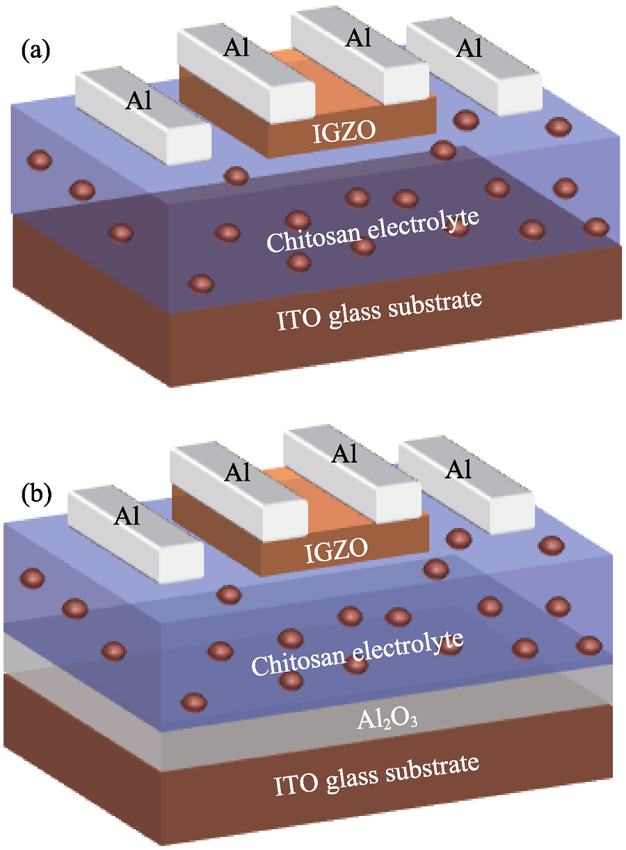
图1 基于不同介质的IGZO神经形态晶体管的结构图
Fig. 1 Schematic diagram of the IGZO-based neuromorphic transistor with different gate dielectrics (a) Chitosan gate dielectric; (b) Stacked Al2O3/chitosan gate dielectrics

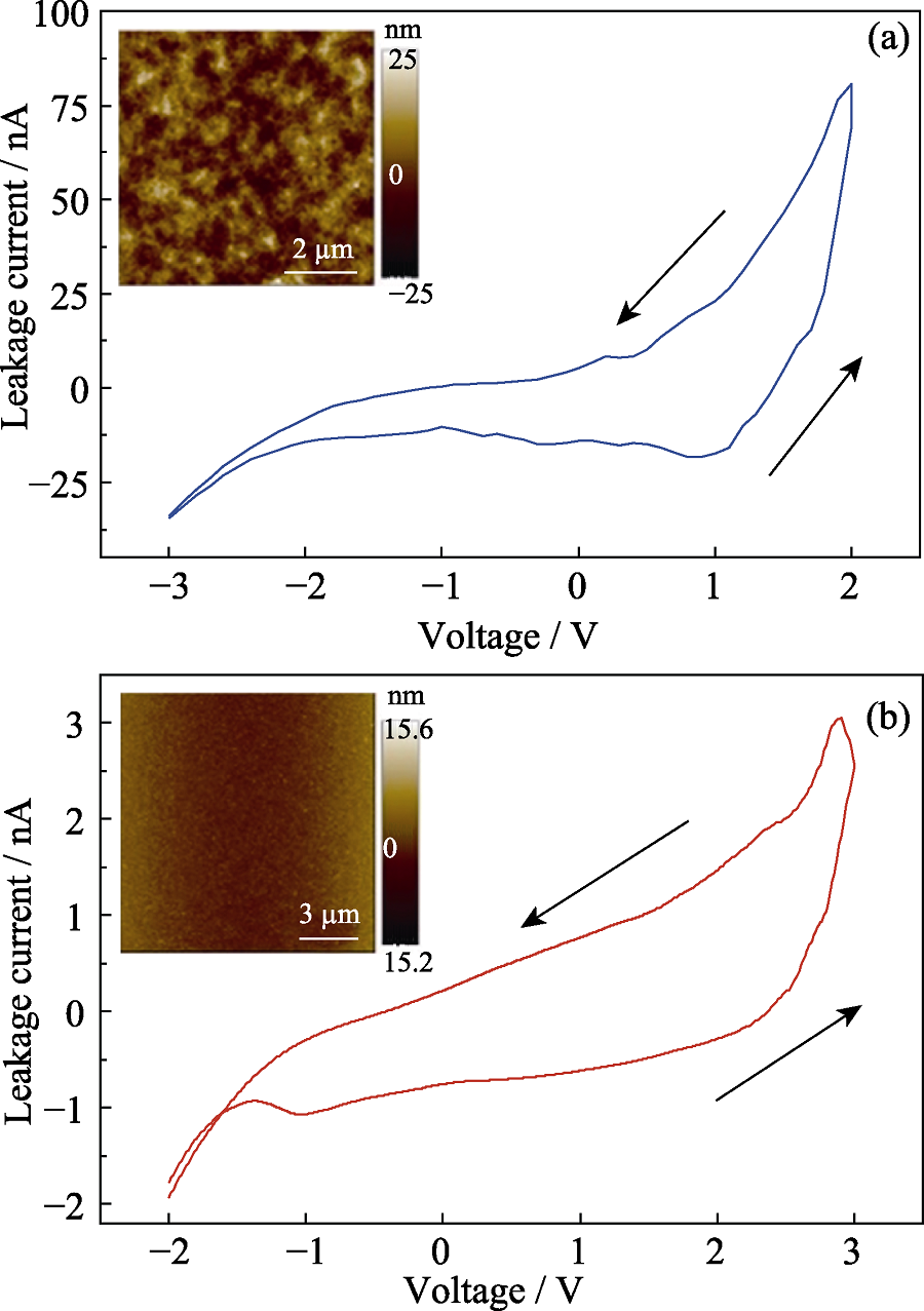
图2 单层、双层栅介质的漏电流曲线及其AFM形貌(插图)
Fig. 2 Leakage current curves and corresponding AFM images (inset) of monolayer gate dielectric and bilayer gate dielectric (a) Chitosan solid dielectric; (b) Stacked Al2O3/chitosan bilayer gate dielectric (Inset: AFM image of Al2O3 membrane)

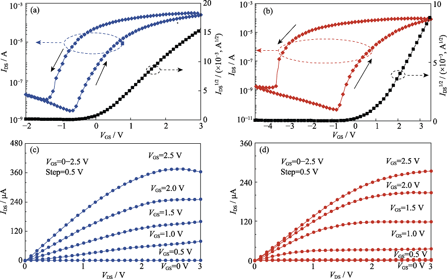
图3 两组不同结构IGZO晶体管的转移曲线和输出曲线
Fig. 3 Transfer characteristics and output characteristics of two kinds of dielectric devices (a,b) Transfer characteristics of chitosan dielectric device (a) and stacked Al2O3/chitosan bilayer gate dielectric device (b); (c) Output characteristic of chitosan dielectric device; (d) Output characteristic of stacked Al2O3/chitosan bilayer gate dielectric device
| Gate dielectric | Ioff | Ion/Ioff ratio | Subthreshold swing/ (mV·decade-1) | Hysteresis window/V | Leakage current (VG=1.8 V)/nA | μsat/ (cm2·V-1·s-1) |
|---|---|---|---|---|---|---|
| Chitosan | 2.92×10⁻⁹ | 1.06×10⁵ | 98.8 | 1.10 | 66.4 | 18.0 |
| Chitosan/Al2O3 | 4.20×10⁻¹¹ | 2.20×10⁶ | 78.3 | 3.73 | 1.3 | 20.9 |
表1 两组IGZO神经形态晶体管的晶体管参数对比
Table 1 Transistor parameters of IGZO-based transistors
| Gate dielectric | Ioff | Ion/Ioff ratio | Subthreshold swing/ (mV·decade-1) | Hysteresis window/V | Leakage current (VG=1.8 V)/nA | μsat/ (cm2·V-1·s-1) |
|---|---|---|---|---|---|---|
| Chitosan | 2.92×10⁻⁹ | 1.06×10⁵ | 98.8 | 1.10 | 66.4 | 18.0 |
| Chitosan/Al2O3 | 4.20×10⁻¹¹ | 2.20×10⁶ | 78.3 | 3.73 | 1.3 | 20.9 |

图4 晶体管的顶部光学显微镜照片(a), 在不同VG2下(范围为-2.0 V至1.0 V)的晶体管转移曲线(b)及不同VG2下的器件阈值电压变化(c)
Fig. 4 (a) Top micrograph, (b) transfer characteristics with different VG2 (from-2.0 V to 1.0 V) and (c) the Vth with different VG2 of transistor

图5 (a) 生物突触结构示意图以及叠层Al2O3/壳聚糖栅介质突触晶体管的等效电路图, (b) 0.5 V, 20 ms电脉冲下的两组器件的EPSC响应, (c) 叠层Al2O3/壳聚糖栅介质晶体管在不同振幅的电脉冲诱发的EPSC
Fig. 5 (a) Schematic diagram of biological synapse and their equivalent electrical circuit of the neuromorphic transistor, (b) EPSC responses under an electric pulse of 0.5 V, and (c) EPSC induced by electric pulses of different amplitudes for IGZO-based dual-gate transistor with stacked Al2O3/chitosan gate dielectrics
| Structure | VDS/V | VG pulse | EPSC/nA | Energy consumption/(pJ·spike-1) | Ref. |
|---|---|---|---|---|---|
| Nanogranular SiO2/IZO | 1.0 | 0.8 V, 20 ms | 5000 | 105 | [ |
| GO+Chitosan/IGZO | 0.1 | 0.5 V, 20 ms | 14 | 28 | [ |
| Carbon Nanotube (CNT) | 0.5 | 4.0 V, 1.0 ms | 15 | 7.5 | [ |
| Chitosan/IZO | 0.1 | 0.5 V, 25 ms | 2.6 | 6.5 | [ |
| Chitosan/IWO | 0.1 | 0.2 V, 20 ms | 4.7 | 9.4 | [ |
| Chitosan/IGZO | 0.1 | 0.5 V, 20 ms | 26 | 52 | [ |
| Tungsten oxide | 0.3 | 0.6 V, 70 ms | 3.8 | 79 | [ |
| Chitosan/ IGZO | 0.1 | 0.5 V, 20 ms | 24 | 48 | This work |
| Chitosan/Al2O3/IGZO | 0.1 | 0.5 V, 20 ms | 0.86 | 1.7 | This work |
表2 不同结构的人工突触晶体管的EPSC能耗对比
Table 2 Energy consumption of the single EPSC peak in different artificial synaptic transistors
| Structure | VDS/V | VG pulse | EPSC/nA | Energy consumption/(pJ·spike-1) | Ref. |
|---|---|---|---|---|---|
| Nanogranular SiO2/IZO | 1.0 | 0.8 V, 20 ms | 5000 | 105 | [ |
| GO+Chitosan/IGZO | 0.1 | 0.5 V, 20 ms | 14 | 28 | [ |
| Carbon Nanotube (CNT) | 0.5 | 4.0 V, 1.0 ms | 15 | 7.5 | [ |
| Chitosan/IZO | 0.1 | 0.5 V, 25 ms | 2.6 | 6.5 | [ |
| Chitosan/IWO | 0.1 | 0.2 V, 20 ms | 4.7 | 9.4 | [ |
| Chitosan/IGZO | 0.1 | 0.5 V, 20 ms | 26 | 52 | [ |
| Tungsten oxide | 0.3 | 0.6 V, 70 ms | 3.8 | 79 | [ |
| Chitosan/ IGZO | 0.1 | 0.5 V, 20 ms | 24 | 48 | This work |
| Chitosan/Al2O3/IGZO | 0.1 | 0.5 V, 20 ms | 0.86 | 1.7 | This work |

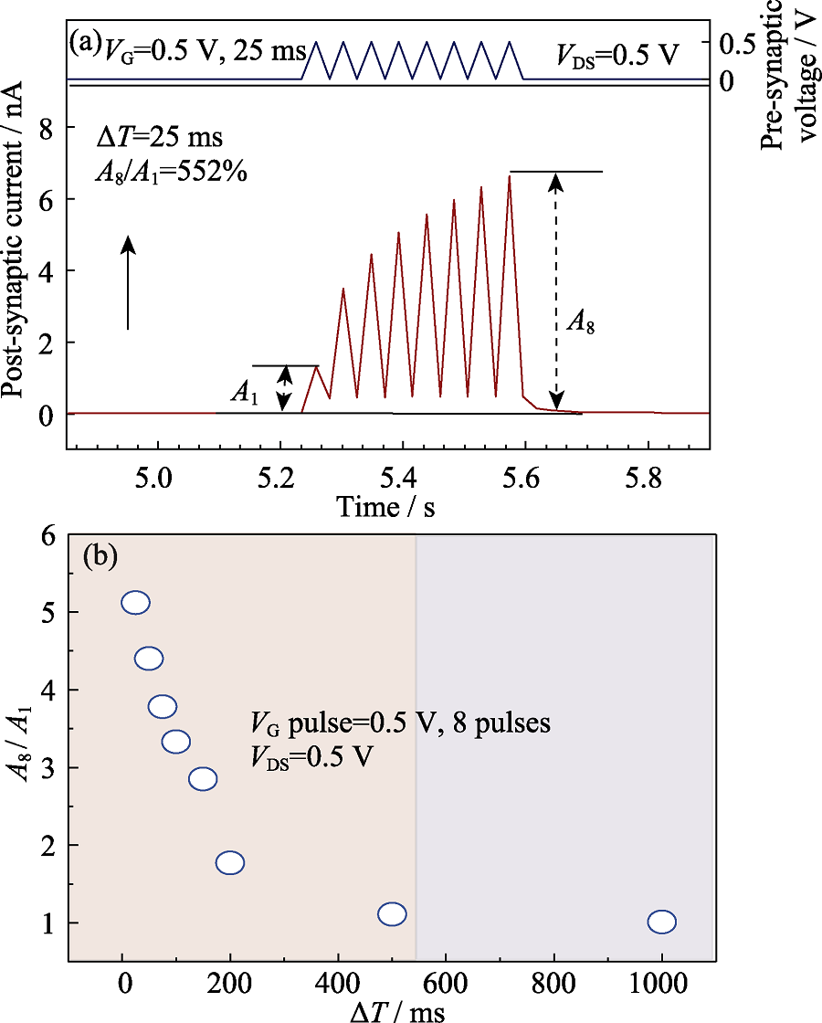
图6 叠层Al2O3/壳聚糖栅介质晶体管的(a)八个连续电脉冲(0.5 V, 25 ms)激发的多脉冲易化现象和(b) A8/A1的比值与脉冲时间间隔的关系图
Fig. 6 (a) Multi-pulse facilitation induced by eight successive electric pulse (0.5 V, 25 ms) and (b) ratio of A8/A1 plotted as a function of the time interval between the pulses for IGZO-based dual-gate transistor with stacked Al2O3/chitosan gate dielectrics
| [1] |
ROY K, JAISWAL A, PANDA P. Towards spike-based machine intelligence with neuromorphic computing. Nature, 2019, 575(7784):607.
DOI |
| [2] |
YU S. Neuro-inspired computing with emerging nonvolatile memorys. Proceedings of the IEEE, 2018, 106(2):260.
DOI URL |
| [3] |
PREZIOSO M, MERRIKH-BAYAT F, HOSKINS B D, et al. Training and operation of an integrated neuromorphic network based on metal-oxide memristors. Nature, 2015, 521(7550):61.
DOI |
| [4] |
ZHU Y, ZHU Y, MAO H, et al. Recent advances in emerging neuromorphic computing and perception devices. Journal of Physics D: Applied Physics, 2021, 55(5):053002.
DOI |
| [5] |
YOU Z, RAMANATHAN S. Mott memory and neuromorphic devices. Proceedings of the IEEE, 2015, 103(8):1289.
DOI URL |
| [6] |
WANG J, LI Y, YIN C, et al. Long-term depression mimicked in an IGZO-based synaptic transistor. IEEE Electron Device Letters, 2017, 38(2):191.
DOI URL |
| [7] | PARK Y J, KWON H T, KIM B, et al. 3-D stacked synapse array based on charge-trap flash memory for implementation of deep neural networks. IEEE Transactions on Electron Devices, 2019, 66(1): 420. |
| [8] | YAN W, PAGE A, NGUYEN-DANG T, et al. Advanced multimaterial electronic and optoelectronic fibers and textiles. Advanced Materials, 2019, 31(1):e1802348. |
| [9] |
YAN W, QU Y, GUPTA T D, et al. Semiconducting nanowire-based optoelectronic fibers. Advanced Materials, 2017, 29(27):1700681.
DOI URL |
| [10] | GKOUPIDENIS P, KOUTSOURAS D A, LONJARET T, et al. Orientation selectivity in a multi-gated organic electrochemical transistor. Scientific Reports, 2016, 6: 27007. |
| [11] |
KIM M K, LEE J S. Ferroelectric analog synaptic transistors. Nano Letters, 2019, 19(3): 2044.
DOI URL |
| [12] | ZHU Y, MAO H, ZHU Y, et al. Photoelectric synapse based on InGaZnO nanofibers for high precision neuromorphic computing. IEEE Electron Device Letters, 2022, 43(4): 651. |
| [13] |
MAO H, HE Y, CHEN C, et al. A spiking stochastic neuron based on stacked InGaZnO memristors. Advanced Electronic Materials, 2021, 8(2):2100918.
DOI URL |
| [14] |
JIANG J, WAN Q, SUN J, et al. Ultralow-voltage transparent electric-double-layer thin-film transistors processed at room-temperature. Applied Physics Letters, 2009, 95 (15): 152114.
DOI URL |
| [15] |
VAN DE BURGT Y, MELIANAS A, KEENE S T, et al. Organic electronics for neuromorphic computing. Nature Electronics, 2018, 1(7):386.
DOI |
| [16] |
HE Y, YANG Y, NIE S, et al. Electric-double-layer transistors for synaptic devices and neuromorphic systems. Journal of Materials Chemistry C, 2018, 6(20):5336.
DOI URL |
| [17] |
HE Y, NIE S, LIU R, et al. Dual-functional long-term plasticity emulated in IGZO-based photoelectric neuromorphic transistors. IEEE Electron Device Letters, 2019, 40(5):818.
DOI URL |
| [18] |
KIM J, KIM Y, KWON O, et al. Modulation of synaptic plasticity mimicked in Al nanoparticle-embedded IGZO synaptic transistor. Advanced Electronic Materials, 2020, 6(4):1901072.
DOI URL |
| [19] |
ZHU Y, HE Y, JIANG S, et al. Indium-gallium-zinc-oxide thin-film transistors: materials, devices, and applications. Journal of Semiconductors, 2021, 42(3):031101.
DOI |
| [20] |
JANG Y, PARK J, KANG J, et al. Amorphous InGaZnO (a-IGZO) synaptic transistor for neuromorphic computing. ACS Applied Electronic Materials, 2022, 4(4):1427.
DOI URL |
| [21] |
VAN DE BURGT Y, LUBBERMAN E, FULLER E J, et al. A non-volatile organic electrochemical device as a low-voltage artificial synapse for neuromorphic computing. Nature Materials, 2017, 16(4):414.
DOI PMID |
| [22] |
KUZUM D, JEYASINGH R G, LEE B, et al. Nanoelectronic programmable synapses based on phase change materials for brain-inspired computing. Nano Letters, 2012, 12(5): 2179.
DOI PMID |
| [23] |
KIM C, FACCHETTI A, MARKS T J. Gate dielectric microstructural control of pentacene film growth mode and field-effect transistor performance. Advanced Materials, 2007, 19(18):2561.
DOI URL |
| [24] |
WANG B, HUANG W, CHI L, et al. High-k gate dielectrics for emerging flexible and stretchable electronics. Chemical Reviews, 2018, 118(11):5690.
DOI URL |
| [25] |
ZHOU J, LIU Y, SHI Y, et al. Solution-processed chitosan-gated IZO-based transistors for mimicking synaptic plasticity. IEEE Electron Device Letters, 2014, 35(2):280.
DOI URL |
| [26] |
GAO S, ZHOU Q, LIU X, et al. Breakdown enhancement and current collapse suppression in AlGaN/GaN HEMT by NiOX/ SiNX and Al2O3/SiNX as gate dielectric layer and passivation layer. IEEE Electron Device Letters, 2019, 40(12): 1921.
DOI URL |
| [27] |
WEI W, ZENG Z, LIAO W, et al. Extended gate ion-sensitive field-effect transistors using Al2O3/hexagonal boron nitride nanolayers for ph sensing. ACS Applied Nano Materials, 2019, 3(1):403.
DOI URL |
| [28] | PALASANTZAS G, HOSSON J D, and BARNAS J. Surface/ interface roughness effects on magneto-electrical properties of thin films. Surface Science, 2002, 507-510: 541. |
| [29] |
LI J, WU J, LIU J, et al. Effect of composition, interface, and deposition sequence on electrical properties of nanolayered Ta2O5-Al2O3 films grown on silicon by atomic layer deposition. Nanoscale Research Letters, 2019, 14(1):75.
DOI |
| [30] |
CHOE M, JO G, MAENG J, et al. Electrical properties of ZnO nanowire field effect transistors with varying high-k Al2O3 dielectric thickness. Journal of Applied Physics, 2010, 107(3):034504.
DOI URL |
| [31] | FORTUNATO E, BARQUINHA P, MARTINS R. Oxide semiconductor thin-film transistors: a review of recent advances. Advanced Materials, 2012, 24(22): 2945. |
| [32] |
ZHU L Q, CHAO J Y, XIAO H, et al. Chitosan-based electrolyte gated low voltage oxide transistor with a coplanar modulatory terminal. IEEE Electron Device Letters, 2017, 38(3):322.
DOI URL |
| [33] |
WAN X, HE Y, NIE S, et al. Biological band-pass filtering emulated by oxide-based neuromorphic transistors. IEEE Electron Device Letters, 2018, 39(11):1764.
DOI URL |
| [34] |
NIE S, HE Y, LIU R, et al. Low-voltage oxide-based synaptic transistors for spiking humidity detection. IEEE Electron Device Letters, 2019, 40(3):459.
DOI URL |
| [35] | KIM K, CHEN C L, TRUONG Q, et al. A carbon nanotube synapse with dynamic logic and learning. Advanced Materials, 2013, 25(12): 1693. |
| [36] |
JIANG S, HE Y, LIU R, et al. Synaptic metaplasticity emulation in a freestanding oxide-based neuromorphic transistor with dual in-plane gates. Journal of Physics D: Applied Physics, 2021, 54(18):185106.
DOI |
| [37] |
LIU R, HE Y, JIANG S, et al. Synaptic plasticity and classical conditioning mimicked in single indium-tungsten-oxide based neuromorphic transistor. Chinese Physics B, 2021, 30(5):058102.
DOI |
| [38] |
ZHANG C, LI S, HE Y, et al. Oxide synaptic transistors coupled with triboelectric nanogenerators for bio-inspired tactile sensing application. IEEE Electron Device Letters, 2020, 41(4):617.
DOI URL |
| [39] | YANG J T, GE C, DU J Y, et al. Artificial synapses emulated by an electrolyte-gated tungsten-oxide transistor. Advanced Materials, 2018, 30(34):e1801548. |
| [40] |
ZIEGLER M, KOHLSTEDT H. Mimic synaptic behavior with a single floating gate transistor: a memflash synapse. Journal of Applied Physics, 2013, 114(19):194506.
DOI URL |
| [1] | 方仁瑞, 任宽, 郭泽钰, 徐晗, 张握瑜, 王菲, 张培文, 李悦, 尚大山. 基于氧化物基电解质栅控晶体管突触的关联学习[J]. 无机材料学报, 2023, 38(4): 399-405. |
| [2] | 杨洋, 崔航源, 祝影, 万昌锦, 万青. 柔性神经形态晶体管研究进展[J]. 无机材料学报, 2023, 38(4): 367-377. |
| [3] | 李 曼, 刘保亭, 王玉强, 王宽冒. 快速退火对 Ni-Al-O 栅介质结构和介电性能的影响[J]. 无机材料学报, 2011, 26(3): 257-260. |
| [4] | 方泽波,谭永胜,朱燕艳,陈圣,蒋最敏. 非晶Er2O3高 k栅介质薄膜的制备及结构特性研究[J]. 无机材料学报, 2008, 23(2): 357-360. |
| 阅读次数 | ||||||
|
全文 |
|
|||||
|
摘要 |
|
|||||