无机材料学报 ›› 2023, Vol. 38 ›› Issue (3): 329-334.DOI: 10.15541/jim20220646
王志强1( ), 吴济安1, 陈昆峰1(), 薛冬峰2()
收稿日期:2022-11-01
修回日期:2022-11-30
出版日期:2023-01-17
网络出版日期:2023-01-17
通讯作者:
陈昆峰, 教授. E-mail: Kunfeng.Chen@sdu.edu.cn;作者简介:王志强(1998-), 男, 硕士. E-mail: wangzhiqiang@mail.sdu.edu.cn
WANG Zhiqiang1(), WU Ji’an1, CHEN Kunfeng1(), XUE Dongfeng2()
Received:2022-11-01
Revised:2022-11-30
Published:2023-01-17
Online:2023-01-17
Contact:
CHEN Kunfeng, professor. E-mail: Kunfeng.Chen@sdu.edu.cn;About author:WANG Zhiqiang (1998-), male, Master. E-mail: wangzhiqiang@mail.sdu.edu.cn
Supported by:摘要:
Er3+和Yb3+共掺杂的YAG晶体是一种非常重要的光学晶体, 目前, 该晶体已经广泛应用于高功率固体激光器, 但是采用提拉法生长大尺寸、低缺陷的掺杂YAG晶体仍然面临很多挑战。本工作采用快速提拉法成功获得了直径为80 mm、长度为230 mm的Er3+和Yb3+共掺杂的YAG单晶。采用不同测试方法评价其结构、掺杂浓度、光吸收、发光性能和刻蚀缺陷。晶片不同位置的拉曼峰峰位以及半峰宽没有明显变化, 说明晶片中心和边缘部分的晶体结构和应变是均匀的。刻蚀结果表明, 腐蚀坑均匀分布在整个腐蚀表面上, 没有观察到位错腐蚀坑特征, 这意味着晶体接近完美。Er3+和Yb3+在不同波长下的强发光峰以及辉光放电质谱结果证明Er,Yb:YAG单晶中成功掺杂了稀土离子。本工作采用提拉法成功生长了大尺寸、低缺陷的Er,Yb:YAG单晶, 证实了快速生长方法对YAG晶体中掺杂双稀土离子是有效的。
中图分类号:
王志强, 吴济安, 陈昆峰, 薛冬峰. 大尺寸Er,Yb:YAG单晶的生长及其性能[J]. 无机材料学报, 2023, 38(3): 329-334.
WANG Zhiqiang, WU Ji’an, CHEN Kunfeng, XUE Dongfeng. Large-size Er,Yb:YAG Single Crystal: Growth and Performance[J]. Journal of Inorganic Materials, 2023, 38(3): 329-334.
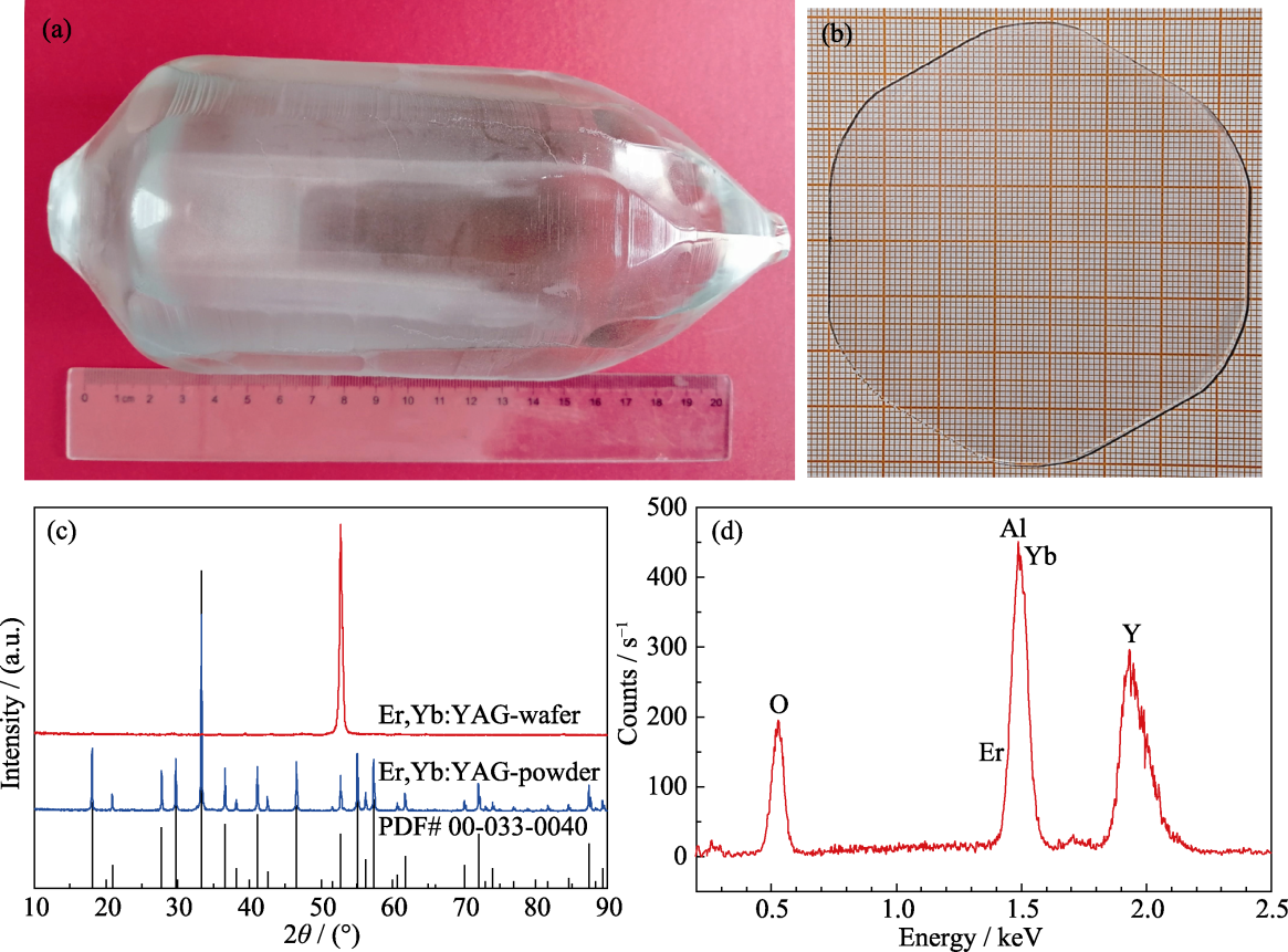
Fig. 1 Characteristics of as-grown Er,Yb:YAG single crystal and wafer (a) With diameter of 80 mm and length of 230 mm; (b) Wafer with a thickness of 1.5 mm; (c) XRD patterns for wafer and ground powder; (d) EDS pattern of the wafer
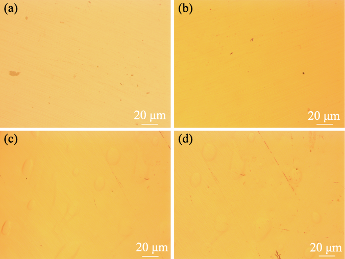
Fig. 2 Micrographs of wafer surface with (111) face (a, b) Before etching; (c, d) Etched in H3PO4 at 180 ℃ for 60 min
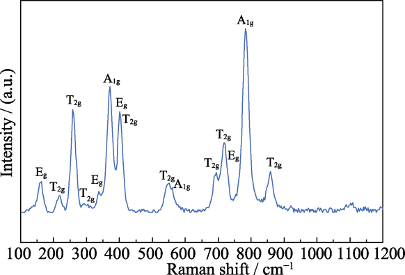
Fig. 3 Raman spectrum of Er,Yb:YAG
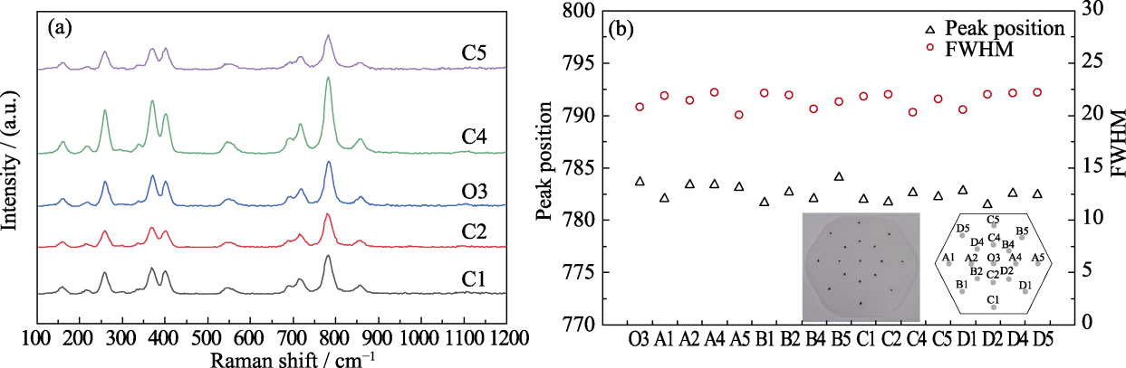
Fig. 4 Raman spectra of different points at Er,Yb:YAG wafer (a) Five points on a straight line; (b) Peak positions and FWHM obtained by Lorentz fitting at the 783 cm-1 band with nisets showing Er,Yb:YAG wafer and schematic diagram of Raman test points
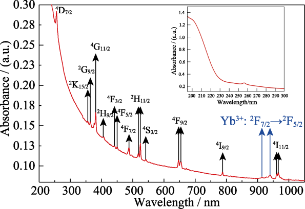
Fig. 5 Optical absorption spectra of Er,Yb:YAG crystal in the range of 200-1050 nm at room temperature
| Wavelength/nm | Assignment (from ground 4I15/2) |
|---|---|
| 255 | 4D7/2 |
| 356 | 2K15/2 |
| 364 | 2G9/2 |
| 381 | 4G11/2 |
| 407 | 2H9/2 |
| 442 | 4F3/2 |
| 450 | 4F5/2 |
| 488 | 4F7/2 |
| 518, 524 | 2H11/2 |
| 542 | 4S3/2 |
| 647, 655 | 4F9/2 |
| 788 | 4I9/2 |
| 961, 966 | 4I11/2 |
Table 1 Correspondence between the experimentally observed absorption lines and energy levels of Er3+ in Er,Yb:YAG single crystal[11,33⇓⇓ -36]
| Wavelength/nm | Assignment (from ground 4I15/2) |
|---|---|
| 255 | 4D7/2 |
| 356 | 2K15/2 |
| 364 | 2G9/2 |
| 381 | 4G11/2 |
| 407 | 2H9/2 |
| 442 | 4F3/2 |
| 450 | 4F5/2 |
| 488 | 4F7/2 |
| 518, 524 | 2H11/2 |
| 542 | 4S3/2 |
| 647, 655 | 4F9/2 |
| 788 | 4I9/2 |
| 961, 966 | 4I11/2 |
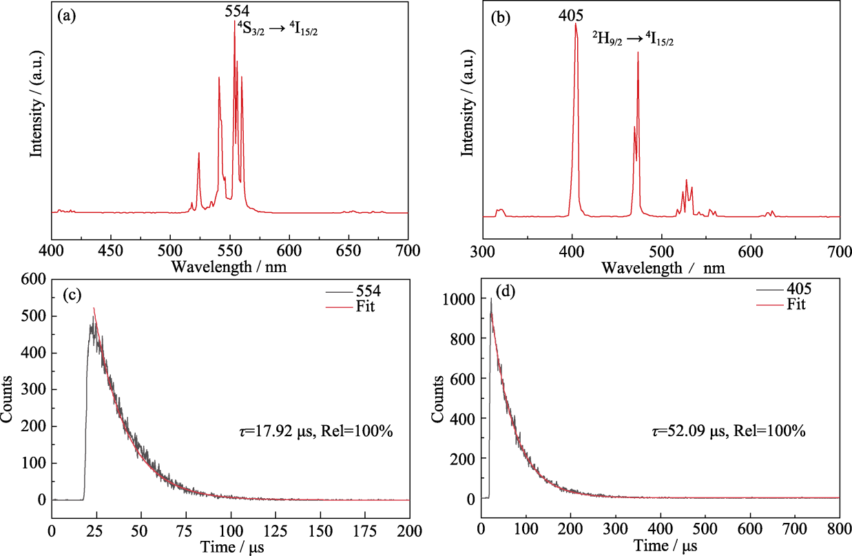
Fig. 6 Emission spectra of Er,Yb:YAG crystal at room temperature (a) Excited by 382 nm; (b) Excited by 260 nm; Fluorescent decay curves of (c) 554 nm; (d) 405 nm emission; Colorful figures are available on website
| [1] |
MA X G, LI X Y, LI J Q, et al. Pressureless glass crystallization of transparent yttrium aluminum garnet-based nanoceramics. Nature Communications, 2018, 9(1): 1175.
DOI PMID |
| [2] |
SUN C T, XUE D. Study on the crystallization process of function inorganic crystal materials. Scientia Sinica Technologica, 2014, 44(11): 1123.
DOI URL |
| [3] |
SUN C T, XUE D. Chemical bonding in micro-pulling down process: high throughput single crystal growth. Science China Technological Sciences, 2018, 61(11): 1776.
DOI |
| [4] |
CHUBB D L, PAL A M T, PATTON M O, et al. Rare earth doped yttrium aluminum garnet (YAG) selective emitters. Materials & Design, 2001, 22(7): 591.
DOI URL |
| [5] |
UPASANI M, BUTEY B, MOHARIL S V. Photoluminescence study of rare earth doped yttrium aluminum garnet-YAG:RE (RE: Eu3+, Pr3+ and Tb3+). Optik, 2016, 127(4): 2004.
DOI URL |
| [6] |
GEORGIOU E, MUSSET O, BOQUILLON J P, et al. 50 mJ/30 ns FTIR Q-switched diode-pumped Er:Yb:glass 1.54 μm laser. Optics Communications, 2001, 198(1/2/3): 147.
DOI URL |
| [7] | MIERCZYK Z, KWASNY M, KOPCZYNSKI K, et al. Er3+ and Yb3+ doped active media for ‘Eye-Safe’ laser systems. Journal of Alloys and Compounds 2020, 300(1): 398. |
| [8] | YANG G, HAN J, LI X, et al. Growth of 8 inch Yb:YAG single crystal by Czochralski method. Journal of Synthetic Crystals, 2019, 48: 1216. |
| [9] |
BAO R J, YU L, YE L H, et al. Compact and sensitive Er3+/Yb3+ co-doped YAG single crystal optical fiber thermometry based on up-conversion luminescence. Sensors and Actuators A: Physical, 2018, 269: 182.
DOI URL |
| [10] | GUO Y, HUANG L, ZHOU J, et al. Czochralski growth and investigation on the photoluminescence properties of YAG:Er single crystal. Journal of Synthetic Crystals, 2019, 48: 24. |
| [11] |
NIZHANKOVSKYI S V, KOZLOVSKYI A A, KOVALENKO N O, et al. Optical and luminescence properties of Er,Yb:YAG crystals grown by horizontal directional crystallization method. Functional Materials, 2019, 26(1): 35.
DOI URL |
| [12] |
SUN C T, XUE D. Chemical bonding theory of single crystal growth and its application to ϕ3'' YAG bulk crystal. CrystEngComm, 2014, 16(11): 2129.
DOI URL |
| [13] |
SUN C T, XUE D. Crystal growth: an anisotropic mass transfer process at the interface. Physical Chemistry Chemical Physics, 2017, 19(19): 12407.
DOI PMID |
| [14] |
YANG P Z, DENG P Z, XU J, et al. Growth of high-quality single crystal of 30at% Yb:YAG and its laser performance. Journal of Crystal Growth, 2000, 216(1-4): 348.
DOI URL |
| [15] |
XU X D, ZHAO Z W, SONG P X, et al. Growth of high-quality single crystal of 50at% Yb:YAG and its spectral properties. Journal of Alloys and Compounds, 2004, 364(1/2): 311.
DOI URL |
| [16] |
XU X D, ZHAO Z W, WANG H H, et al. Spectroscopic and thermal properties of Cr,Yb:YAG crystal. Journal of Crystal Growth, 2004, 262(1-4): 317.
DOI URL |
| [17] |
ZHU M D, QI H J, PAN M Y, et al. Growth and luminescent properties of Yb:YAG and Ca co-doped Yb:YAG ultrafast scintillation crystals. Journal of Crystal Growth, 2018, 490: 51.
DOI URL |
| [18] |
BOGAERTS A, GIJBELS R. New developments and applications in GDMS. Fresenius Journal of Analytical Chemistry, 1999, 364(5): 367.
DOI URL |
| [19] |
DI SABATINO M. Detection limits for glow discharge mass spectrometry (GDMS) analyses of impurities in solar cell silicon. Measurement, 2014, 50: 135.
DOI URL |
| [20] |
YANG P Z, DENG P Z, YIN Z W, et al. The growth defects in Czochralski-grown Yb:YAG crystal. Journal of Crystal Growth, 2000, 218(1): 87.
DOI URL |
| [21] |
YIN H B, DENG P Z, GAN F X. Defects in YAG:Yb crystals. Journal of Applied Physics, 1998, 83(7): 3825.
DOI URL |
| [22] |
HURRELL J P, PORTO S P S, CHANG I F, et al. Optical phonons of yttrium aluminum garnet. Physical Review, 1968, 173(3): 851.
DOI URL |
| [23] |
PAPAGELIS K, KANELLIS G, VES S, et al. Lattice dynamical properties of the rare earth aluminum garnets (RE3Al5O12). Physica Status Solidi B-Basic Solid State Physics, 2002, 233(1): 134.
DOI URL |
| [24] |
CHEN Y F, LIM P K, LIM S J, et al. Raman scattering investigation of Yb:YAG crystals grown by the Czochralski method. Journal of Raman Spectroscopy, 2003, 34(11): 882.
DOI URL |
| [25] |
PAPAGELIS K, KANELLIS G, ARVANITIDIS J, et al. Phonons in rare-earth aluminum garnets and their relation to lattice vibration of AlO4. Physica Status Solidi B-Basic Research, 1999, 215(1): 193.
DOI URL |
| [26] |
QIU H W, YANG P Z, DONG J, et al. The influence of Yb concentration on laser crystal Yb:YAG. Materials Letters, 2002, 55(1/2): 1.
DOI URL |
| [27] |
WANG T, ZHANG J, ZHANG N, et al. The characteristics of high-quality Yb:YAG single crystal fibers grown by a LHPG method and the effects of their discoloration. RSC Advances, 2019, 9(39): 22567.
DOI URL |
| [28] |
WANG X D, XU X D, ZENG X H, et al. Effects of Yb concentration on the spectroscopic properties of Yb:Y3Al5O12. Spectrochimica Acta Part A-Molecular and Biomolecular Spectroscopy, 2006, 63(1): 49.
DOI URL |
| [29] |
WANG X D, XU X D, ZHAO Z W, et al. Comparison of fluorescence spectra of Yb:Y3Al5O12 and Yb:YAlO3 single crystals. Optical Materials, 2007, 29(12): 1662.
DOI URL |
| [30] | GUERASSIMOVA N, GARNIER N, DUJARDIN C, et al. X-ray-excited charge transfer luminescence in YAG:Yb and YbAG. Journal of Luminescence, 2001, 94: 11. |
| [31] |
ZORENKO Y, GORBENKO V, SAVCHYN V, et al. Luminescence properties and energy transfer processes in YAG:Yb,Er single crystalline films. Radiation Measurements, 2013, 56: 134.
DOI URL |
| [32] |
SARDAR D K, RUSSELL C C, GRUBER J B, et al. Absorption intensities and emission cross sections of principal intermanifold and inter-stark transitions of Er3+ (4f11) in polycrystalline ceramic garnet Y3Al5O12. Journal of Applied Physics, 2005, 97(12): 123501.
DOI URL |
| [33] |
BURDICK G W, GRUBER J B, NASH K L, et al. Analyses of 4f11 energy levels and transition intensities between stark levels of Er3+ in Y3Al5O12. Spectroscopy Letters, 2010, 43(5): 406.
DOI URL |
| [34] |
ZHOU J, ZHANG W X, WANG L, et al. Fabrication, microstructure and optical properties of polycrystalline Er3+:Y3Al5O12 ceramics. Ceramics International, 2011, 37(1): 119.
DOI URL |
| [35] |
SEKITA M, HANEDA H, SHIRASAKI S, et al. Optical spectra of undoped and rare‐earth‐(=Pr, Nd, Eu, and Er) doped transparent ceramic Y3Al5O12. Journal of Applied Physics, 1991, 69(6): 3709.
DOI URL |
| [36] |
NIZHANKOVSKYI S V, KOZLOVSKYI A A, KOVALENKO N O, et al. Spectral properties of Er-doped yttrium aluminum garnet crystals grown by modified horizontal directional crystallization method. Functional Materials, 2018, 25(4): 646.
DOI URL |
| [37] |
BI F, DONG X T, WANG J X, et al. Facile electrospinning preparation and up-conversion luminescence performance of Y3Al5O12:Er3+,Yb3+ nanobelts. Journal of Inorganic and Organometallic Polymers and Materials, 2014, 24(2): 407.
DOI URL |
| [38] |
KATARIA V, MEHTA D S. Investigation of concurrent emissions in visible, UV and NIR region in Gd2O2S:Er,Yb nanophosphor by diverse excitation wavelengths as a function of firing temperature. Optical Materials, 2019, 95: 109204.
DOI URL |
| [1] | 马玲玲, 常江. Nd掺杂硅酸钙及其复合电纺丝膜的制备及性能研究[J]. 无机材料学报, 2021, 36(9): 974-980. |
| [2] | 戴云, 张中晗, 苏良碧, 李金, 龙勇, 丁雨憧, 武安华. 激光加热基座法生长高质量Yb3+掺杂Y3Al5O12单晶光纤[J]. 无机材料学报, 2021, 36(7): 761-765. |
| [3] | 杨金萍, 季文玲, 张浩, 刘盼, 崔燚, 魏恒勇. Eu 3+掺杂的多孔锆酸镧粉体制备及发光性能研究[J]. 无机材料学报, 2019, 34(7): 727-733. |
| [4] | 曾祥雄, 杨进超, 左联, 杨奔奔, 秦峻, 彭志航. Li/Ce/La共掺杂对CaBi2Nb2O9陶瓷晶体结构及电学性能的影响[J]. 无机材料学报, 2019, 34(4): 379-386. |
| [5] | 张庆福, 李 臣, 宋志国, 李永进, 邱建备, 杨正文. F/Cl比对卤磷酸钙固溶体Bi离子掺杂位点及价态的调控[J]. 无机材料学报, 2017, 32(6): 661-666. |
| [6] | 吴 霜, 刘 波, 陈士伟, 张娟楠, 刘小林, 顾 牡, 黄世明, 倪 晨, 薛超凡. Lu2SiO5: Ce3+透明薄膜制备及其发光性能研究[J]. 无机材料学报, 2016, 31(9): 948-954. |
| [7] | 毛启楠, 李 鹤, 季振国, 席俊华, 张 峻, 孔 哲. Eu2+和Dy3+掺杂浓度对Sr2MgSi2O7材料的荧光和长余辉性能的影响[J]. 无机材料学报, 2016, 31(8): 819-826. |
| [8] | 吴 霜, 刘 波, 邱志澈, 陈士伟, 张娟楠, 刘小林, 顾 牡, 黄世明, 倪 晨. LuTaO4:Ln3+(Ln=Eu,Tb)透明薄膜制备改进与其发光性能研究[J]. 无机材料学报, 2016, 31(4): 372-376. |
| [9] | 张志雄, 欧阳绍业, 张约品, 夏海平. 白光LED用Ba2LaF7: Pr3+微晶玻璃的发光性能研究[J]. 无机材料学报, 2016, 31(10): 1046-1050. |
| [10] | 王运锋, 宋金璠, 唐晓燕, 胡冬梅. NaGd(WO4)2:Yb3+/Tm3+反蛋白石光子晶体的制备与上转换发光调制研究[J]. 无机材料学报, 2016, 31(10): 1058-1062. |
| [11] | 殷海荣, 刘 晶, 乔荫颇, 李艳肖, 张 攀, 周 沁, 杨 晨. 锶含量对稀土Eu掺杂锶钙羟基磷灰石发光性能及取代位置的影响[J]. 无机材料学报, 2016, 31(10): 1103-1109. |
| [12] | 张书娴, 崔 博, 王宏志, 李耀刚, 张青红. 柔性Eu3+掺杂SiO2纳米纤维薄膜的制备及其发光性能[J]. 无机材料学报, 2015, 30(7): 719-724. |
| [13] | 彭 霞, 李淑星, 刘学建,黄毅华, 黄政仁, 李会利. Eu2+/Tb3+掺杂的Sr2Si5N8基荧光粉的制备与发光性能[J]. 无机材料学报, 2015, 30(4): 397-400. |
| [14] | 李金生, 孙旭东, 李晓东, 刘绍宏, 朱 琦. 硬脂酸盐熔融法合成(Y,Lu)AG:Ce荧光粉及荧光性能研究[J]. 无机材料学报, 2015, 30(2): 177-182. |
| [15] | 彭 霞, 李淑星, 刘学建, 黄政仁, 李会利. Sr2Si5N8:Eu2+荧光粉的制备及其发光性能研究[J]. 无机材料学报, 2014, 29(12): 1281-1286. |
| 阅读次数 | ||||||
|
全文 |
|
|||||
|
摘要 |
|
|||||