无机材料学报 ›› 2022, Vol. 37 ›› Issue (10): 1109-1115.DOI: 10.15541/jim20220030
所属专题: 【能源环境】量子点
张可忆1( ), 郑琦1(), 王连军1, 江莞1,2()
收稿日期:2021-01-18
修回日期:2022-02-22
出版日期:2022-10-20
网络出版日期:2022-07-08
通讯作者:
江莞, 教授. E-mail: wanjiang@dhu.edu.cn;作者简介:张可忆(1997-), 男, 硕士研究生. E-mail: zhangkeyiwork@outlook.com
基金资助:
ZHANG Keyi1(), ZHENG Qi1(), WANG Lianjun1, JIANG Wan1,2()
Received:2021-01-18
Revised:2022-02-22
Published:2022-10-20
Online:2022-07-08
Contact:
JIANG Wan, professor. E-mail: wanjiang@dhu.edu.cn;About author:ZHANG Keyi (1997-), male, Master candidate. E-mail: zhangkeyiwork@outlook.com
Supported by:摘要:
制备硒化银(Ag2Se)薄膜材料对于组装微型器件至关重要, 目前大部分制备方法难以精确控制薄膜尺寸并进行图案化设计, 喷墨打印技术成为解决这一问题的有效方法, 实现其与Ag2Se材料的组合具有重要意义。本工作通过溶剂热法制备了Ag2Se纳米颗粒, 再与不同分散剂混合以筛选出适用于喷墨打印的稳定墨水, 进一步调节喷射参数以优化打印过程中墨滴的形态, 提高打印质量。将墨水打印至聚酰亚胺衬底上, 经热处理后制备得到Ag2Se薄膜。使用不同手段对其物相与微结构进行表征, 并测试不同打印层数薄膜的电学性能。结果表明: 随着墨水固含量与打印层数增加, Ag2Se薄膜的结晶度和致密度得到明显提升, 电导率也得到相应提高, 这主要源于薄膜内部Ag2Se纳米颗粒沉积量与堆积密集程度增加。当使用固含量为5 mg·mL-1的墨水进行打印, 打印层数为40层时, Ag2Se薄膜的电导率达到399 S·cm-1, 表现出较高的导电性能。本研究为制备Ag2Se基薄膜材料与器件提供了新的方向。
中图分类号:
张可忆, 郑琦, 王连军, 江莞. 用于喷墨打印的Ag2Se墨水的制备及表征[J]. 无机材料学报, 2022, 37(10): 1109-1115.
ZHANG Keyi, ZHENG Qi, WANG Lianjun, JIANG Wan. Preparation and Characterization of Ag2Se-based Ink Used for Inkjet Printing[J]. Journal of Inorganic Materials, 2022, 37(10): 1109-1115.
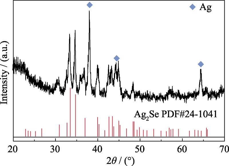
图1 Ag2Se粉体的XRD谱图
Fig. 1 XRD patterns of Ag2Se powders
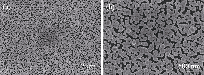
图2 Ag2Se粉体的SEM照片
Fig. 2 SEM images of Ag2Se powder (a) Low-resolution; (b) High-resolution
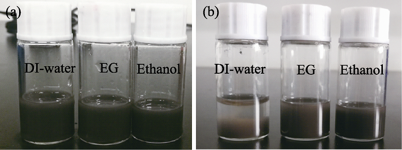
图3 溶剂热法合成的Ag2Se粉体在不同溶剂中的分散性和稳定性
Fig. 3 Dispersion and stability of Ag2Se powders synthesized by solvothermal method in different solvents (a) Optical images of Ag2Se ink after ultrasonic dispersion; (b) 12-h still-standing
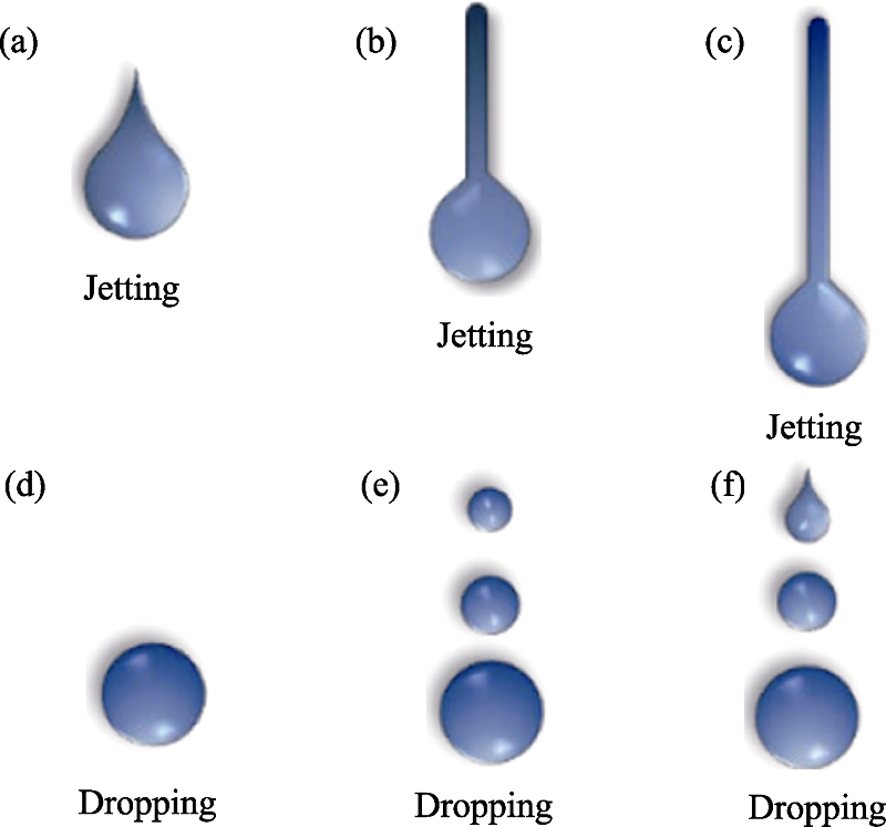
图4 设置不同喷嘴电压时的液滴形态
Fig. 4 Shape of droplets with different cartridge voltage setting (a, d) 18 V; (b, e) 21 V; (c, f) 26 V
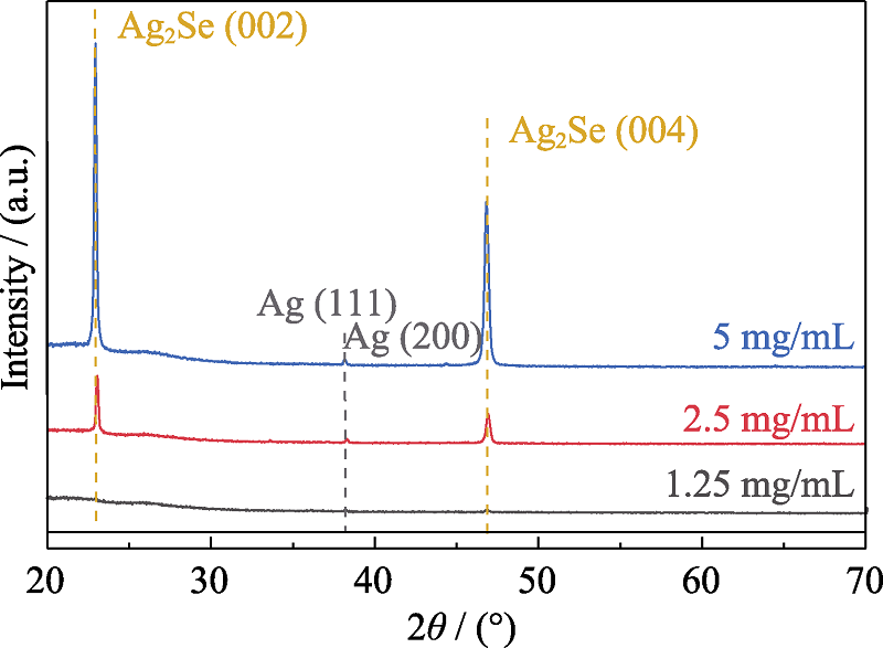
图5 不同固含量墨水打印制备的Ag2Se薄膜的XRD谱图
Fig. 5 XRD patterns of Ag2Se films corresponding to different ink concentrations
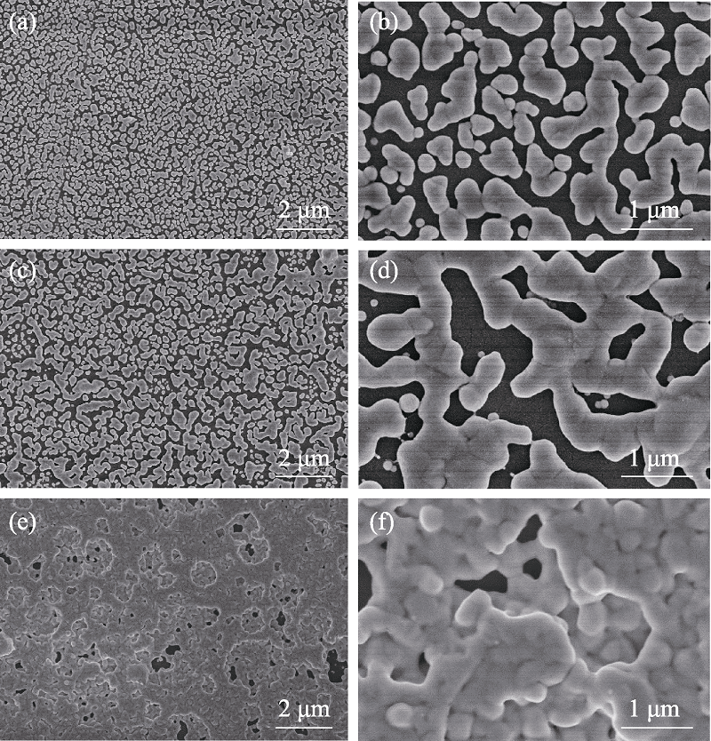
图6 不同固含量墨水打印制备的Ag2Se薄膜的SEM照片
Fig. 6 SEM images of Ag2Se films printed with different ink concentrations (a-b) 1.25 mg·mL-1; (c-d) 2.5 mg·mL-1; (e-f) 5 mg·mL-1
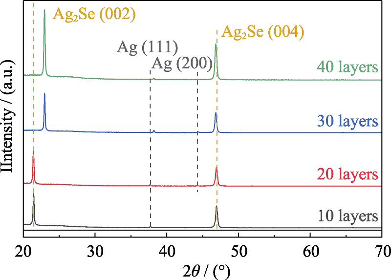
图7 不同打印层数的Ag2Se薄膜的XRD谱图
Fig. 7 XRD patterns of Ag2Se films with different printing layers
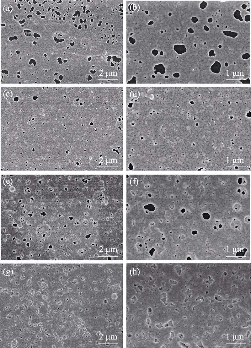
图8 不同打印层数的Ag2Se薄膜的SEM照片
Fig. 8 SEM images of Ag2Se films with different printing layers (a-b) 10 layers; (c-d) 20 layers; (e-f) 30 layers; (g-h) 40 layers
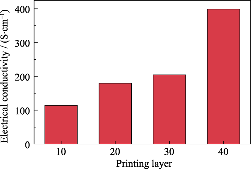
图9 Ag2Se薄膜的电性能与打印层数之间的关系
Fig. 9 Electrical conductivity of Ag2Se films as a function of printing layers

图10 使用喷墨打印工艺印制的图案
Fig. 10 Pattern printed through inkjet printing technology
| [1] |
YANG D, BENTON A, HE J, et al. Novel synthesis recipes boosting thermoelectric study of A2Q (A = Cu, Ag; Q = S, Se, Te). J. Phys. D, 2020, 53(19): 193001.
DOI URL |
| [2] |
XIAO C, XU J, LI K, et al. Superionic phase transition in silver chalcogenide nanocrystals realizing optimized thermoelectric performance. J. Am. Chem. Soc., 2012, 134(9): 4287-4293.
DOI PMID |
| [3] |
YIN X, LI X, ZHU C, et al. Integration of fluorescence/ photoacoustic imaging and targeted chemo/photothermal therapy with Ag2Se@BSA-RGD nanodots. New J. Chem., 2020, 44(12): 4850-4857.
DOI URL |
| [4] |
GU Y P, CUI R, ZHANG Z L, et al. Ultrasmall near-infrared Ag2Se quantum dots with tunable fluorescence for in vivo imaging. J. Am. Chem. Soc., 2012, 134(1): 79-82.
DOI URL |
| [5] |
DONG B H, LI C Y, CHEN G C, et al. Facile synthesis of highly photoluminescent Ag2Se quantum dots as a new fluorescent probe in the second near-infrared window for in vivo imaging. Chem. Mater., 2013, 25(12): 2503-2509.
DOI URL |
| [6] | YANG Y, PAN D Q, ZHANG Z, et al. Photovoltaic performance of Ag2Se quantum dots co-sensitized solid-state dye sensitized solar cells. J. Inorg. Mater., 2019, 2(34): 137-144. |
| [7] |
JOOD P, CHETTY R, OHTA M. Structural stability enables high thermoelectric performance in room temperature Ag2Se. J. Mater. Chem. A, 2020, 8(26): 13024-13037.
DOI URL |
| [8] |
LEE C, PARK Y H, HASHIMOTO H. Effect of nonstoichiometry on the thermoelectric properties of a Ag2Se alloy prepared by a mechanical alloying process. J. Appl. Phys., 2007, 101(2): 024920.
DOI URL |
| [9] |
MI W, QIU P, ZHANG T, et al. Thermoelectric transport of Se-rich Ag2Se in normal phases and phase transitions. Appl. Phys. Lett., 2014, 104(13): 133903.
DOI URL |
| [10] |
ZHANG Q H, BAI S Q, CHEN L D. Technologies and applications of thermoelectric devices: current status, challenges and prospects. J. Inorg. Mater., 2019, 34(3): 279-293.
DOI URL |
| [11] |
MANOHARAN S S, PRASANNA S J, KIWITZ D E, et al. Magnetoresistance in microwave synthesized Ag2+θSe (0.0≤θ≤0.2). Phys. Rev., B, 2001, 63(21): 212405.
DOI URL |
| [12] | ZHU H M, YUE S. Magnetoresistance effect of silver selenide thin films fabricated by magnetron sputtering. J. Cryst. Growth, 2014, 43(11): 2892-2896. |
| [13] |
GAO J, MIAO L, LAI H, et al. Thermoelectric flexible silver selenide films: compositional and length optimization. iScience, 2020, 23(1): 100753.
DOI URL |
| [14] |
JIANG C, DING Y, CAI K, et al. Ultrahigh performance of n-type Ag2Se films for flexible thermoelectric power generators. ACS Appl. Mater. Interfaces, 2020, 12(8): 9646-9655.
DOI URL |
| [15] |
JIANG C, WEI P, DING Y, et al. Ultrahigh performance polyvinylpyrrolidone/Ag2Se composite thermoelectric film for flexible energy harvesting. Nano Energy, 2020, 80: 105488.
DOI URL |
| [16] |
HOU S, LIU Y, YIN L, et al. High performance wearable thermoelectric generators using Ag2Se films with large carrier mobility. Nano Energy, 2021, 87: 106223.
DOI URL |
| [17] |
JINDAL S, SINGH S, SAINI G S S, et al. Enhanced thermopower in (013)-oriented silver selenide films produced by thermal annealing. Appl. Phys. A, 2020, 126(5): 374-387.
DOI URL |
| [18] |
DAMODARA D V, KARUNAKARAN D. Thermoelectric power of annealed β-Ag2Se alloy thin films: Temperature and size effects-possibility of a new (β2) phase at low temperatures. J. Appl. Phys., 1990, 67(2): 878-883.
DOI URL |
| [19] |
DING Y, QIU Y, CAI K, et al. High performance n-type Ag2Se film on Nylon membrane for flexible thermoelectric power generator. Nat. Commun., 2019, 10(1): 841-847.
DOI URL |
| [20] |
ZHOU K, CHEN J, ZHENG R, et al. Non-epitaxial pulsed laser deposition of Ag2Se thermoelectric thin films for near-room temperature applications. Ceram. Int., 2016, 42(10): 12490.
DOI URL |
| [21] |
SHI J Z, WANG H, WERNER J, et al. Study of preparation of BZN ceramic ink. J. Inorg. Mater., 2008, 23(2): 257-261.
DOI URL |
| [22] |
YANG J, PAN Z H, SHENG L M, et al. Graphene nanosheets prepared by arc discharge method and their application in conductive inkjet. J. Inorg. Mater., 2017, 1(32): 39-44.
DOI URL |
| [23] |
GAO M, LI L, SONG Y. Inkjet printing wearable electronic devices. J. Mater. Chem. C, 2017, 5(12): 2971-2993.
DOI URL |
| [24] |
NAYAK L, MOHANTY S, NAYAK S K, et al. A review on inkjet printing of nanoparticle inks for flexible electronics. J. Mater. Chem. C, 2019, 7(29): 8771-8795.
DOI URL |
| [25] | WANG G X, PEI Z B, YE C H. Inkjet-printing and performance investigation of self-powered flexible graphene oxide humidity sensors. J. Inorg. Mater., 2019, 1(34): 114-120. |
| [26] |
WANG J, FAN W, YANG J, et al. Tetragonal-orthorhombic-cubic phase transitions in Ag2Se nanocrystals. Chem. Mater., 2014, 26(19): 5647-5653.
DOI URL |
| [27] | WANG C C. Analysis and research of the ink-jet printing quality. Packaging Engineering, 2008(2): 55-57. |
| [28] | SONG B, TANG Z Z. Parameter analysis of droplet ejection of piezoelectric ink-jet printing. Packaging Engineering, 2011, 32(19): 93-96. |
| [29] |
CHEN R, XU D, GUO G, et al. Electrodeposition of silver selenide thin films from aqueous solutions. J. Mater. Chem., 2002, 12(5): 1437-1441.
DOI URL |
| [1] | 张国庆, 秦鹏, 黄富强. 空间限域铅离子与钙钛矿纳米晶间的可逆转换与信息存储应用[J]. 无机材料学报, 2022, 37(4): 445-451. |
| [2] | 李榅凯, 赵宁, 毕志杰, 郭向欣. 钠离子电池Na3Zr2Si2PO12陶瓷电解质的喷雾干燥法制备及性能优化[J]. 无机材料学报, 2022, 37(2): 189-196. |
| [3] | 樊帅, 金天, 张山林, 雒晓涛, 李成新, 李长久. Li2O烧结助剂对固体氧化物燃料电池LSGM电解质烧结特性及离子电导率的影响[J]. 无机材料学报, 2022, 37(10): 1087-1092. |
| [4] | 杨英,潘德群,张政,陈甜,韩晓敏,张力松,郭学益. Ag2Se量子点共敏化固态染料敏化太阳能电池光电性能研究[J]. 无机材料学报, 2019, 34(2): 137-144. |
| [5] | 施徐国, 李明远, 马维刚, 周新贵, 张兴. KD-II型碳化硅纤维热输运性质的实验研究[J]. 无机材料学报, 2018, 33(7): 756-760. |
| [6] | 穆阳, 邓佳欣, 李皓, 周万城. 两种连续SiC纤维的高温介电及吸波性能对比[J]. 无机材料学报, 2018, 33(4): 427-433. |
| [7] | 卢东亮, 代广周, 姚英邦, 陶涛, 梁波, 鲁圣国. 煅烧温度对Li0.33La0.56TiO3固态离子电容器性能的影响[J]. 无机材料学报, 2018, 33(10): 1077-1082. |
| [8] | 南 辉, 王文利, 韩建华, 尹学文, 周 宇, 赵晓冲, 林 红. 基于FeI2/Ni2+溶液还原制备低成本的高导电性及催化性 纸张石墨[J]. 无机材料学报, 2017, 32(9): 997-1003. |
| [9] | 唐慧丽, 吴庆辉, 罗 平, 王庆国, 徐 军. In:Ga2O3氧化物半导体晶体的生长与性能研究[J]. 无机材料学报, 2017, 32(6): 621-624. |
| [10] | 刘勇英, 仇鹏飞, 陈弘毅, 陈瑞, 史迅, 陈立东. 基于离子阻挡法测量电子-离子混合导体中离子电导率的研究[J]. 无机材料学报, 2017, 32(12): 1337-1344. |
| [11] | 曹珍珠, 任 伟, 刘进荣, 李国荣, 高艳芳, 房明浩, 何伟艳. Sb掺杂Li7La3Zr2O12陶瓷的显微结构及离子导电性能研究[J]. 无机材料学报, 2014, 29(2): 220-224. |
| [12] | 孙 琳, 卢 军, 殷洁炜, 尹屹梅, 马紫峰. 新型SOFC阳极材料La0.75Sr0.25Mn0.5Cr0.5-xCuxO3-δ的合成与表征[J]. 无机材料学报, 2013, 28(9): 925-930. |
| [13] | 顾媛媛, 陈 康, 江 浩, 简家文. La0.9Sr0.1Ga0.8Mg0.2Ox固体电解质材料敏感电学特性的研究[J]. 无机材料学报, 2013, 28(4): 409-414. |
| [14] | 章志珍, 施思齐, 胡勇胜, 陈立泉. 溶胶-凝胶法制备钠离子固态电解质Na3Zr2Si2PO12及其电导性能研究[J]. 无机材料学报, 2013, 28(11): 1255-1260. |
| [15] | 靳宏建, 王 欢, 张 华, 金 江. 甘氨酸-硝酸盐法合成GdBaCo2O5+δ阴极材料及其性能[J]. 无机材料学报, 2012, 27(7): 751-756. |
| 阅读次数 | ||||||
|
全文 |
|
|||||
|
摘要 |
|
|||||