无机材料学报 ›› 2020, Vol. 35 ›› Issue (6): 682-688.DOI: 10.15541/jim20190386
所属专题: 【虚拟专辑】层状MAX,MXene及其他二维材料
谭仕林,尹顺达,欧阳钢( )
)
收稿日期:2019-07-22
修回日期:2019-08-19
出版日期:2020-06-20
网络出版日期:2019-09-04
作者简介:谭仕林(1994-), 男, 硕士研究生. E-mail: tanshilin_hnu@126.com; 基金资助:
TAN Shilin,YIN Shunda,OUYANG Gang()
Received:2019-07-22
Revised:2019-08-19
Published:2020-06-20
Online:2019-09-04
Supported by:摘要:
为探索界面工程对二维材料范德华异质结构中载流子复合率的影响, 本工作基于界面键弛豫理论和费米黄金定则, 建立了范德华异质结俄歇和层间复合率与各结构组元尺寸之间的理论模型。结果表明, MoS2/WSe2异质结的俄歇复合寿命随着组元尺寸的增大而增加, 且异质结的俄歇复合率远小于相应的单组元体系。在MoS2/WSe2双层异质结中引入薄h-BN插层后, 体系的层间复合率和俄歇复合率随h-BN厚度的增加而分别呈现减小和增大的趋势; 在组元处于单层MoS2和WSe2情况下, 当界面插层h-BN厚度达到9.1 nm时, 俄歇复合率将趋于5.3 ns -1。该研究结果为二维过渡金属硫族化合物基异质结光电器件的优化设计提供了一种理论依据。
中图分类号:
谭仕林,尹顺达,欧阳钢. 尺寸效应对MoS2/WSe2范德华异质结构层间与俄歇复合的界面调控[J]. 无机材料学报, 2020, 35(6): 682-688.
TAN Shilin,YIN Shunda,OUYANG Gang. Size Effect on the Interface Modulation of Interlayer and Auger Recombination Rates in MoS2/WSe2 van der Waals Heterostructures[J]. Journal of Inorganic Materials, 2020, 35(6): 682-688.
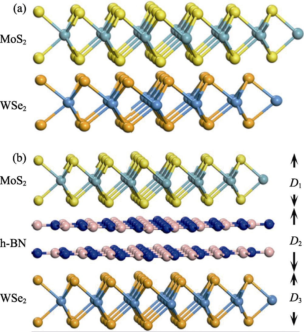
图1 (a) MoS2/WSe2和(b) MoS2/h-BN/WSe2两种不同范德华异质结构示意图 (a) MoS2/WSe2; (b) MoS2/h-BN/WSe2
Fig. 1 Schematic diagrams of two kinds of van der Waals heterostructures
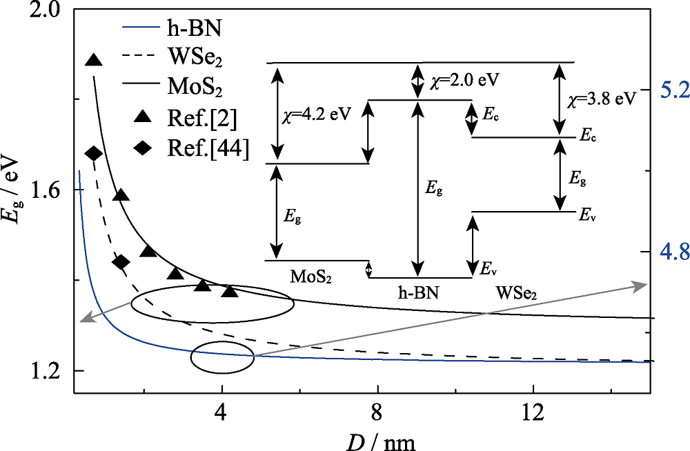
图2 厚度依赖的MoS2、WSe2和h-BN的带隙
Fig. 2 Thickness-dependent bandgaps of MoS2, WSe2 and h-BN
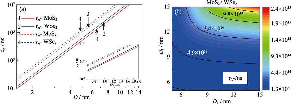
图3 不同体系的厚度依赖的负俄歇复合寿命(${{\tau }_{{{\text{A}}^{-}}}}$)和双激子俄歇复合寿命(${{\tau }_{{{\text{A}}^{xx}}}}$)
Fig. 3 Thickness-dependent AR lifetime of negative trion (${{\tau }_{{{\text{A}}^{-}}}}$) and biexciton (${{\tau }_{{{\text{A}}^{xx}}}}$) of different system (a) Single component system MoS2 and WSe2; (b) MoS2/WSe2 heterostructures Inset shows the ${{\tau }_{\text{A}}}$under the condition of D<2.0 nm
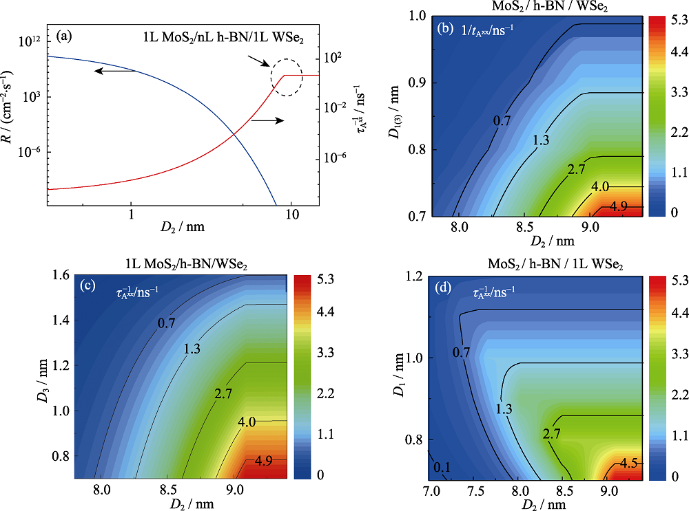
图4 厚度依赖的异质结层间(R)和双激子俄歇复合率($\tau _{{{\text{A}}^{xx}}}^{-1}$)
Fig. 4 Thickness-dependent interlayer recombination (R) and biexciton AR rate ($\tau _{{{\text{A}}^{xx}}}^{-1}$) of heterostructures (a) Monolayer MoS2/h-BN/Monolayer WSe2; (b) MoS2/h-BN/WSe2; (c) Monolayer MoS2/h-BN/WSe2; (d) MoS2/h-BN/Monolayer WSe2
| [1] | LI M Y, CHEN C H, SHI Y , et al. Heterostructures based on two-dimensional layered materials and their potential applications. Mater. Today, 2016,19(6):322-335. |
| [2] | MAK K F, LEE C, HONE J , et al. Atomically thin MoS2: a new direct-gap semiconductor. Phys. Rev. Lett., 2010,105(13):136805. |
| [3] | XIAO M, SUN R Z, LI Y F , et al. Transfer printing of VO2 thin films using MoS2/SiO2 van der Waals heterojunctions. J. Inorg. Mater., 2019,34(11):1161-1166. |
| [4] | ZHAO Y, YU W, OUYANG G . Size-tunable band alignment and optoelectronic properties of transition metal dichalcogenide van der Waals heterostructures. J. Phys. D: Appl. Phys., 2017,51(1):015111. |
| [5] | CAO G, SHANG A, ZHANG C , et al. Optoelectronic investigation of monolayer MoS2/WSe2 vertical heterojunction photoconversion devices. Nano Energy, 2016,30:260-266. |
| [6] |
FURCHI M M, ZECHMEISTER A A, HOELLER F , et al. Photovoltaics in van der Waals heterostructures. IEEE J. Sel. Top. Quantum Electron., 2016,23(1):106-116.
DOI URL |
| [7] | CHEN Q, LI Q, YANG Y , et al. Effects of AlGaN interlayer on scattering mechanisms in InAlN/AlGaN/GaN heterostructures. Acta Phys. Sin., 2019,68(1):017301. |
| [8] | FANG H, BATTAGLIA C, CARRARO C , et al. Strong interlayer coupling in van der Waals heterostructures built from single-layer chalcogenides. Proc. Natl. Acad. Sci., 2014,111(17):6198-6202. |
| [9] | LATINI S, WINTHER K T, OLSEN T , et al. Interlayer excitons and band alignment in MoS2/h-BN/WSe2 van der Waals heterostructures. Nano Lett., 2017,17(2):938-945. |
| [10] | KIM J Y, KIM S G, YOUN J W , et al. Energy and charge transfer effects in two-dimensional van der Waals hybrid nanostructures on periodic gold nanopost array. Appl. Phys. Lett., 2018,112(19):193101. |
| [11] | YANG L, YU X, XU M , et al. Interface engineering for efficient and stable chemical-doping-free graphene-on-silicon solar cells by introducing a graphene oxide interlayer. J. Mater. Chem. A, 2014,2(40):16877-16883. |
| [12] | MENG J H, LIU X, ZHANG X W , et al. Interface engineering for highly efficient graphene-on-silicon Schottky junction solar cells by introducing a hexagonal boron nitride interlayer. Nano Energy, 2016,28:44-50. |
| [13] | SUN W F, LI M C, ZHAO L C . First-principles investigation of carrier Auger lifetime and impact ionization rate in narrow-gap superlattices. Acta Phys. Sin., 2010,59(8):5661-5666. |
| [14] | HE Y, OUYANG G . Geometry-dependent Auger recombination process in semiconductor nanostructures. J. Phys. Chem. C, 2017,121(42):23811-23816. |
| [15] | 贺言 . 半导体纳米结构的表/界面以及光电性质的调控研究. 长沙: 湖南师范大学博士学位论文, 2017. |
| [16] | LI Q, LIAN T . Area- and thickness-dependent biexciton Auger recombination in colloidal CdSe nanoplatelets: breaking the “universal volume scaling law”. Nano Lett., 2017,17(5):3152-3158. |
| [17] | LIU S D, CHENG M T, ZHOU H J , et al. The effect of biexciton, wetting layer leakage and Auger capture on Rabi oscillation damping in quantum dots. Acta Phys. Sin., 2006,55(5):2122-2127. |
| [18] | DENNIS A M, MANGUM B D, PIRYATINSKI A , et al. Suppressed blinking and Auger recombination in near-infrared type-II InP/CdS nanocrystal quantum dots. Nano Lett., 2012,12(11):5545-5551. |
| [19] | PARK Y S, BAE W K, PADILHA L A , et al. Effect of the core/shell interface on Auger recombination evaluated by single-quantum-dot spectroscopy. Nano Lett., 2014,14(2):396-402. |
| [20] |
JAIN A, VOZNYY O, HOOGLAND S , et al. Atomistic design of CdSe/CdS core-shell quantum dots with suppressed Auger recombination. Nano Lett., 2016,16(10):6491-6496.
DOI URL |
| [21] | VAXENBURG R, RODINA A, LIFSHITZ E , et al. Biexciton Auger recombination in CdSe/CdS core/shell semiconductor nanocrystals. Nano Lett., 2016,16(4):2503-2511. |
| [22] |
PELTON M, ANDREWS J J, FEDIN I , et al. Nonmonotonic dependence of Auger recombination rate on shell thickness for CdSe/CdS core/shell nanoplatelets. Nano Lett., 2017,17(11):6900-6906.
DOI URL |
| [23] | BEATTIE A R, LANDSBERG P T . Auger effect in semiconductors. Proc. R. Soc. London. Ser. A, 1959,249(1256):16-29. |
| [24] |
LU N, GUO H, WANG L , et al. Van der Waals trilayers and superlattices: modification of electronic structures of MoS2 by intercalation. Nanoscale, 2014,6(9):4566-4571.
DOI URL |
| [25] |
SUN C Q . Size dependence of nanostructures: impact of bond order deficiency. Prog. Solid State Chem., 2007,35(1):1-159.
DOI URL |
| [26] |
OUYANG G, WANG C X, YANG G W . Surface energy of nanostructural materials with negative curvature and related size effects. Chem. Rev., 2009,109(9):4221-4247.
DOI URL |
| [27] | ZHANG A, ZHU Z, HE Y , et al. Structure stabilities and transitions in polyhedral metal nanocrystals: an atomic-bond-relaxation approach. Appl. Phys. Lett., 2012,100(17):171912. |
| [28] | ZHU Z, ZHANG A, OUYANG G , et al. Edge effect on band gap shift in Si nanowires with polygonal cross-sections. Appl. Phys. Lett., 2011,98(26):263112. |
| [29] |
CHEPIC D I, EFROS A L, EKIMOV A I , et al. Auger ionization of semiconductor quantum drops in a glass matrix. J. Lumin., 1990,47(3):113-127.
DOI URL |
| [30] |
OUYANG G, ZHU W G, SUN C Q , et al. Atomistic origin of lattice strain on stiffness of nanoparticles. Phys. Chem. Chem. Phys., 2010,12(7):1543-1549.
DOI URL |
| [31] |
DANOVICH M, ZÓLYOMI V, FAL’KO V I, et al. Auger recombination of dark excitons in WS2 and WSe2 monolayers. 2D Materials, 2016,3(3):035011.
DOI URL |
| [32] |
JIN C, KIM J, WU K , et al. On optical dipole moment and radiative recombination lifetime of excitons in WSe2. Adv. Funct. Mater., 2017,27(19):1601741.
DOI URL |
| [33] |
HUR J H, PARK J, JEON S . A theoretical modeling of photocurrent generation and decay in layered MoS2 thin-film transistor photosensors. J. Phys. D: Appl. Phys., 2017,50(6):065105.
DOI URL |
| [34] |
GUO N, WEI J, JIA Y , et al. Fabrication of large area hexagonal boron nitride thin films for bendable capacitors. Nano Research, 2013,6(8):602-610.
DOI URL |
| [35] | KIRCHARTZ T, MATTHEIS J, RAU U . Detailed balance theory of excitonic and bulk heterojunction solar cells. Phys. Rev. B, 2008,78(23):235320. |
| [36] |
ZEGRYA G G, ANDREEV A D . Mechanism of suppression of Auger recombination processes in type-II heterostructures. Appl. Phys. Lett., 1995,67(18):2681-2683.
DOI URL |
| [37] |
HE Y, QUAN J, OUYANG G . The atomistic origin of interface confinement and enhanced conversion efficiency in Si nanowire solar cells. Phys. Chem. Chem. Phys., 2016,18(10):7001-7006.
DOI URL |
| [38] |
ZHANG C, FU L, ZHAO S , et al. Controllable Co-segregation synthesis of wafe-scale hexagonal boron nitride thin films. Adv. Mater., 2014,26(11):1776-1781.
DOI URL |
| [39] |
KANG J, TONGAY S, ZHOU J , et al. Band offsets and heterostructures of two-dimensional semiconductors. Appl. Phys. Lett., 2013,102(1):012111.
DOI URL |
| [40] | WANG J, MA F, LIANG W , et al. Optical, photonic and optoelectronic properties of graphene, h-BN and their hybrid materials. Nanophotonics, 2017,6(5):943-976. |
| [41] |
VU Q A, LEE J H, NGUYEN V L , et al. Tuning carrier tunneling in van der Waals heterostructures for ultrahigh detectivity. Nano Lett., 2016,17(1):453-459.
DOI URL |
| [42] |
DAS S, PRAKASH A, SALAZAR R , et al. Towards low-power electronics: tunneling phenomena in transition metal dichalcogenides. ACS Nano, 2014,8(2):1681-1689.
DOI URL |
| [43] | CHOI M S, LEE G H, YU Y J , et al. Controlled charge trapping by molybdenum disulphide and graphene in ultrathin heterostructured memory devices. Nat. Commun., 2013,4(1):1624. |
| [44] | YUN W S, HAN S W, HONG S C , et al. Thickness and strain effects on electronic structures of transition metal dichalcogenides: 2H-MX2 semiconductors (M=Mo, W; X=S, Se, Te). Phys. Rev. B, 2012,85(3):033305. |
| [45] | GARCÍA-SANTAMARÍA F, BROVELLI S, VISWANATHA R , et al. Breakdown of volume scaling in Auger recombination in CdSe/CdS heteronanocrystals: the role of the core-shell interface. Nano Lett., 2011,11(2):687-693. |
| [46] |
COHN A W, RINEHART J D, SCHIMPF A M , et al. Size dependence of negative trion Auger recombination in photodoped CdSe nanocrystals. Nano Lett., 2013,14(1):353-358.
DOI URL |
| [47] |
HE Y, HU S, HAN T , et al. Suppression of the Auger recombination process in CdSe/CdS core/shell nanocrystals. ACS Omega, 2019,4(5):9198-9203.
DOI URL |
| [1] | 吐尔洪·木尼热, 赵红刚, 马玉花, 齐献慧, 李钰宸, 闫沉香, 李佳文, 陈平. 单晶WO3/红磷S型异质结的构建及光催化活性研究[J]. 无机材料学报, 2023, 38(6): 701-707. |
| [2] | 伍林, 胡明蕾, 王丽萍, 黄少萌, 周湘远. TiHAP@g-C3N4异质结的制备及光催化降解甲基橙[J]. 无机材料学报, 2023, 38(5): 503-510. |
| [3] | 王如意, 徐国良, 杨蕾, 邓崇海, 储德林, 张苗, 孙兆奇. p-n异质结BiVO4/g-C3N4光阳极的制备及其光电化学水解性能[J]. 无机材料学报, 2023, 38(1): 87-96. |
| [4] | 马心全, 李喜宝, 陈智, 冯志军, 黄军同. S型异质结BiOBr/ZnMoO4的构建及光催化降解性能研究[J]. 无机材料学报, 2023, 38(1): 62-70. |
| [5] | 李涛, 曹鹏飞, 胡力涛, 夏勇, 陈一, 刘跃军, 孙翱魁. NH4+扩层MoS2的制备及其储锌性能研究[J]. 无机材料学报, 2023, 38(1): 79-86. |
| [6] | 陈士昆, 王楚楚, 陈晔, 李莉, 潘路, 文桂林. 磁性Ag2S/Ag/CoFe1.95Sm0.05O4 Z型异质结的制备及光催化降解性能[J]. 无机材料学报, 2022, 37(12): 1329-1336. |
| [7] | 高娃, 熊宇杰, 吴聪萍, 周勇, 邹志刚. 基于超薄纳米结构的光催化二氧化碳选择性转化[J]. 无机材料学报, 2022, 37(1): 3-14. |
| [8] | 刘彭, 吴仕淼, 吴昀峰, 张宁. Zn0.4(CuGa)0.3Ga2S4/CdS光催化材料的制备及其CO2还原性能[J]. 无机材料学报, 2022, 37(1): 15-21. |
| [9] | 赵宇鹏,贺勇,张敏,史俊杰. 新型二维Zr2CO2/InS异质结可见光催化产氢性能的第一性原理研究[J]. 无机材料学报, 2020, 35(9): 993-998. |
| [10] | 许世超,朱天哲,乔阳,白学健,唐楠,郑春明. Z型BiVO4/GO/g-C3N4复合材料的制备及其可见光下催化性能[J]. 无机材料学报, 2020, 35(7): 839-846. |
| [11] | 林海, 苏玮韬, 朱玉, 彭湃, 冯苗, 于岩. WO3纳米花的热处理晶格调控及WO3/CdS/α-S异质结的构筑[J]. 无机材料学报, 2020, 35(12): 1349-1356. |
| [12] | 张之明,方晓生. ZnO纳米棒/ZnCo2O4纳米片异质结的制备及其光电探测性能[J]. 无机材料学报, 2019, 34(9): 991-996. |
| [13] | 孙超祥, 陈亮, 常宇, 田维, 李亮. 基于p-Se/Al2O3/n-ZnO纳米棒阵列异质结的自驱动紫外-可见光探测器[J]. 无机材料学报, 2019, 34(5): 560-566. |
| [14] | 赵世怀,杨紫博,赵晓明,徐文文,温昕,张庆印. NiCo2S4@ACF异质电极材料的绿色制备及其超级电容性能研究[J]. 无机材料学报, 2019, 34(2): 130-136. |
| [15] | 魏科年, 刘展, 左士祥, 严向玉, 吴凤芹, 李霞章, 姚超, 刘孝恒. 高性能CeO2/片状CdS复合光电极材料的制备及在光阴极保护中应用[J]. 无机材料学报, 2019, 34(12): 1334-1340. |
| 阅读次数 | ||||||
|
全文 |
|
|||||
|
摘要 |
|
|||||