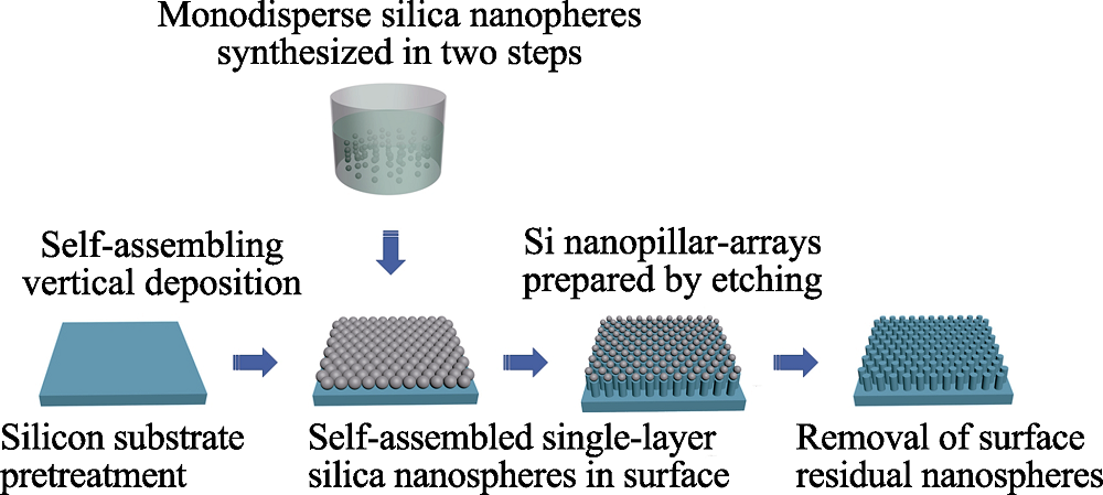
| [1] |
BAZARS F J, LONG J P, GEMSBOK Q J , et al. Mie resonance- enhanced light absorption in periodic silicon nanopillar arrays. Optics Express, 2013,21(23):27587-27601.
DOI
URL
|
| [2] |
KUZNETSOVA A I, MIROSHNICHENKO A E, BRONGERSMA M L , et al. Optically resonant dielectric nanostructures. Science, 2016, 354(6314): 2472-1-8.
|
| [3] |
DECKER M, STAUDE I . Resonant dielectric nanostructures: a low loss platform for functional nanophotonics. Journal of Optics, 2016, 18(10): 103001-1-31.
|
| [4] |
YU RUI, LIN Q F, LEUNG S F , et al. Nanomaterials and nanostructures for efficient light absorption and photovoltaics. Nano Energy, 2012,1(1):57-72.
|
| [5] |
STEWART MATTHEW E, ANDERTON CHRISTOPHER R, THOMPSON LUCAS B , et al. Nanostructured plasmonic sensors. Chem. Rev., 2008,108(2):494-521.
DOI
URL
|
| [6] |
GAO HONGWEI TUNG KAR HOO PATRICK, TENG JINGHUA, , et al. Coupling of surface plasmon with InGaAs/GaAs quantum well emission by gold nanodisk arrays. Applied Optics, 2013,52(16):3698-3702.
DOI
URL
|
| [7] |
GARRELIE F, COLOMBIER J P, PIGEON F , et al. Evidence of surface plasmon resonance in ultrafast laser-induced ripples. Optics Express, 2011,19(10):9035-9043.
DOI
URL
|
| [8] |
KRUK SERGEY and KIVSHAR YURI . Functional meta-optics and nanophotonics governed by Mie resonances. ACS Photonics, 2017,4(11):2638-2649.
DOI
URL
|
| [9] |
KIM E, CHO Y, PARK K T , et al. Mie resonance-mediated antireflection effects of Si nanocone arrays fabricated on 8-in. wafers using a nanoimprint technique. Nano Research Letters, 2015, 10: 164-1-5.
|
| [10] |
FU YUAN HSING, KUZNETSOV ARSENIY I, MIROSHNICHENKO ANDREY E , et al. Directional visible light scattering by silicon nanoparticles. Nature Communications, 2013, 4: 1527-1-6.
|
| [11] |
SPINELLI P, VERSCHOOR M A, POLMAN A . Broadband omnidirectional antireflection coating based on subwavelength surface Mie resonators. Nature Communications, 2012, 3: 692-1-5.
|
| [12] |
GARIN M, FENOLLOSA R, ALCUBILLA R , et al. All-silicon spherical-Mie-resonator photodiode with spectral response in the infrared region. Nature Communications, 2014, 5: 3440-1-6.
|
| [13] |
SPINELLI P, POLMAN A . Light trapping in thin crystalline Si solar cells using surface Mie scatterers. IEEE Journal of Photovoltaics, 2014,4(2):554-559.
DOI
URL
|
| [14] |
BRONGERSMA MARK L, CUI YI , et al. Light management for photovoltaics using high-index nanostructures. Nature Materials, 2014,13:451-460.
|
| [15] |
GARCIA P D, IBISATE M, SAPIENZA R , et al. Mie resonances to tailor random lasers. Physical Review A, 2009, 80(1): 013833- 1-6.
|
| [16] |
SHCHERBAKOV M R, VABISHCHEVICH P P, SHOROKHOV A S , et al. Ultrafast all-optical switching with magnetic resonances in nonlinear dielectric nanostructures. Nano Letters, 2015,15(10):6985-6990.
DOI
URL
|
| [17] |
BOUNDARHAM G, ABDEDDAIM R, BONOD N . Enhancing the magnetic field intensity with a dielectric gap antenna. Applied Physics Letters, 2014, 104(2): 021117-1-4.
|
| [18] |
YAVAS O, SVEDENDAHL M, DOBOSZ P , et al. On-a-chip biosensing based on all-dielectric nanoresonators. Nano Lett., 2017,17(7):4421-4439.
DOI
URL
|
| [19] |
LI R K, TO H, ANDONIAN G , et al. Surface-plasmon resonance- enhanced multiphoton emission of high-brightness electron beams from a nanostructured copper cathode. Physical Review Letters, 2013, 110(7): 074801-1-5.
|
| [20] |
SHEMELYA C, DEMEO D F, VANDERVELDE T E . Two dimensional metallic photonic crystals for light trapping and anti-reflective coatings in thermophotovoltaic applications. Applied Physical Letters, 2014, 104(2): 021115-1-4.
|
| [21] |
KOOY N, MOHAMED K, PIN L T , et al. A review of roll-to-roll nanoimprint lithography. Nanoscale Research Letters, 2014, 9: 320-1-13.
|
| [22] |
LI LUPING, YIN FANG, CHEN XU , et al. Controlling the geometries of Si nanowires through tunable nanosphere lithography. Applied Materials & Interfaces, 2017,9(8):7368-7375.
|
| [23] |
CAI ZHONGYU, SMITH NATASHA L, ZHANG JIAN-TAO , et al. Two-dimensional photonic crystal chemical and biomolecular sensors. Anal. Chem., 2015,87(10):5013-5025.
DOI
URL
|
| [24] |
YANG BO, HE HUI, ZHOU YANGBO , et al. Application of fumed silica to polymer fields. Chemical Industry and Engineering Progress, 2005,24(3):372-377.
|
| [25] |
WANG ZICHEN, WANG LIWEI, ZHAO JINGZHE , et al. Preparation of ultrafine SiO2 powders with large specific surface area. Journal of Inorganic Materials, 1997,12(3):391-396.
|
| [26] |
MOULIK S P, PAUL B K . Uses and applications of microemulsions. Current Science, 2001,80(8):990-1001.
|
| [27] |
WU YIZHI, ZHANG CHENG, YUAN YE , et al. Fabrication of wafer-size monolayer close-packed colloidal crystals via slope self-assembly and thermal treatment. Langmuir, 2013,29(46):14017-14023.
DOI
URL
|
| [28] |
WU C C, HSU C C, LIN Y C , et al. Optical property of an antireflection coating fabricated by an optimal spin-coating method with a pH-modified SiO2 nanoparticle solution. Chinese Optics Letters, 2017,15(2):1671-7694.
|
| [29] |
CHEN S L, DONG P, YANG G H , et al. Characteristic aspects of formation of new particles during the growth of monosize silica seeds. Journal of Colloid and Interface Science, 1996,180(295):237-241.
DOI
URL
|
 ),朱志甫1,邓文娟1