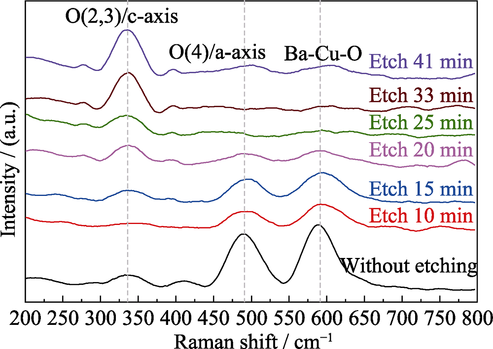
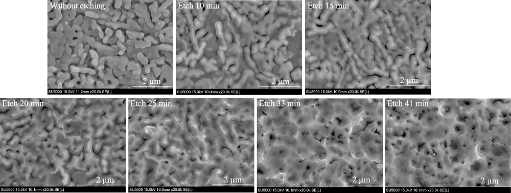
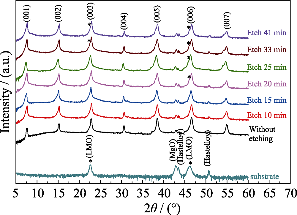
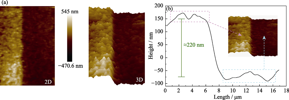
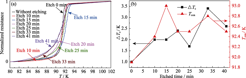
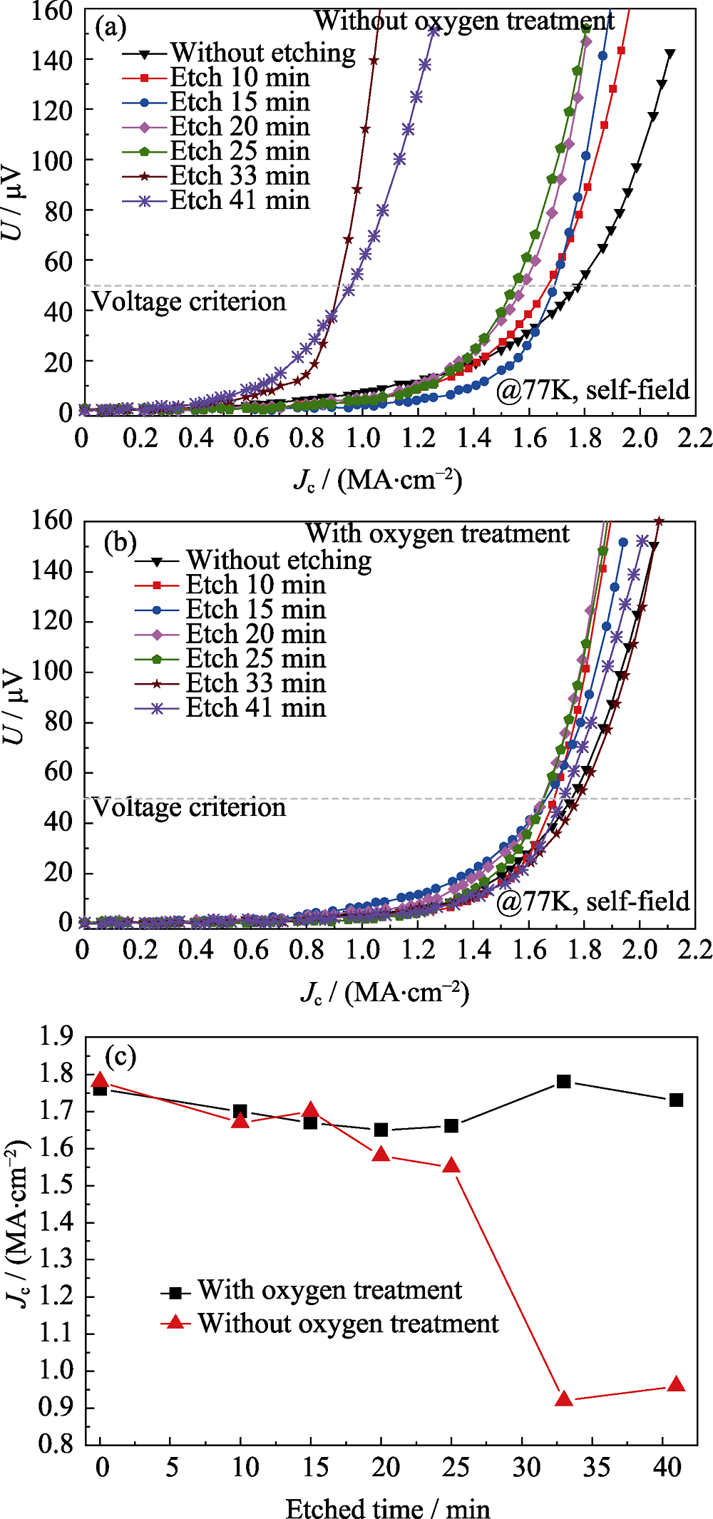
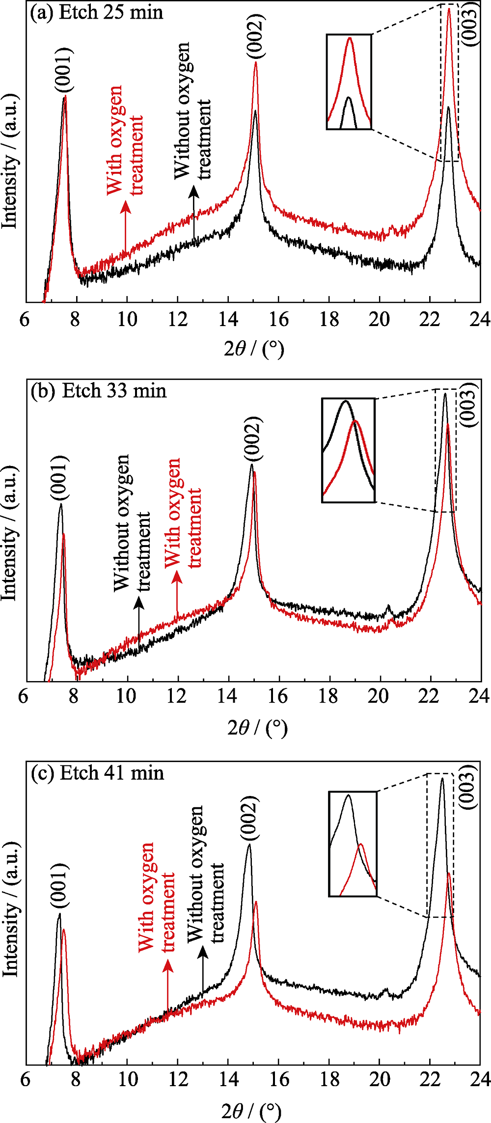
| [1] |
DAVID L, ALEX G, FELDMANN M D , et al. High-Tc superconducting materials for electric power applications. Nature, 2001,414(11):368-377.
|
| [2] |
RUPICH M W, SCHOOP U, VEREBELYI D T , et al. YBCO coated conductors by an MOD/RABiTS process. IEEE Transactions on Applied Superconductivity, 2003,13(2):2458-2461.
|
| [3] |
WANG S S, ZHANG Z L, WANG L , et al. High quality uniform YBCO film growth by the metalorganic deposition using trifluoroacetates. Physica C: Superconductivity and Its Applications, 2017,534:68-72.
|
| [4] |
YAMANE H, KUROSAWA H, HIRAI T . Preparation of YBCO superconducting nano-composite films by MOCVD. Journal of the Japan Society of Powder & Powder Metallurgy, 2009,41(4):370-376.
|
| [5] |
JIANG P, ZHANG S, FAN Z , et al. Development of multipass MOCVD process for fabricating (Gd,Y)Ba2Cu3O7-δ coated conductors. IEEE Transactions on Applied Superconductivity, 2017,27(4):1-5.
|
| [6] |
STADEL O, SCHMIDT J, WAHL G , et al. Continuous YBCO deposition by MOCVD for coated conductors. Physica C: Superconductivity & Its Applications, 2002,372(372):751-754.
|
| [7] |
MATIAS V, HAMMOND R H . YBCO superconductor wire based on IBAD-textured templates and RCE of YBCO:process economics. Physics Procedia, 2012,36:1440-1444.
|
| [8] |
CHOI S M, LEE J W, SHIN G H , et al. Characteristics of high-Jc GdBCO coated conductors fabricated by the RCE-DR process. IEEE Transactions on Applied Superconductivity, 2013,23(3):8001004.
|
| [9] |
SHIN H, DEDICATORIA M J, KIM H . Measurement of electromechanical property in thick-film EDDC-SmBCO coated conductors with high critical current. IEEE Transactions on Applied Superconductivity, 2012,22(1):8400506.
|
| [10] |
ZHANG H, YANG J, LI T , et al. Film thickness dependence of microstructure and superconductive property of PLD prepared YBCO layers. Physica C: Superconductivity & Its Applications, 2014,499(4):54-56.
|
| [11] |
BUSBEE J, BIGGERS R, KOZLOWSKI G , et al. Investigation of in situ Raman spectra for the control of PLD of YBCO thin film superconductors. Engineering Applications of Artificial Intelligence, 2000,13(5):589-596.
|
| [12] |
OHKI K, NAGAISHI T, KATO T , et al. Fabrication, microstructure and persistent current measurement of an intermediate grown superconducting (iGS) joint between REBCO-coated conductors. Superconductor Science and Technology, 2017, 30(11): 115017-1-7.
|
| [13] |
PARK Y, LEE M, ANN H , et al. A superconducting joint for GdBa2Cu3O7-x-coated conductors. NPG Asia Materials, 2014,6(5):e98.
|
| [14] |
JEE Y A, LI M, MA B , et al. Comparison of texture development and superconducting properties of YBCO thin films prepared by TFA and PLD processes. Physica C, 2001,356(4):297-303.
|
| [15] |
NIKOLAY N, BALASHOY, PAVEL N , et al. Low-resistance soldered joints of commercial 2G HTS wire prepared at various values of applied pressure. IEEE Transactions on Appiled Superconductivity, 2018,28(4):6602604.
|
| [16] |
SUNGHO L, WOO I Y, HO S J , et al. The efects of Gd-free impurity phase on the aging behavior for the microwave surface resistance of Ag-coated GdBa2Cu3O7-δ at cryogenic temperatures. Electronic Materials Letters, 2018,14(5):646-654.
|
| [17] |
JORGENSEN J D, VEAL B W, PAULIKAS A P , et al. Structural properties of oxygen-deficient YBa2Cu3O7-δ. Physical Review B Condensed Matter, 1990,41(4):1863-1877.
|
| [18] |
HABERKORN N, GUIMPEL J, SUAREZ S , et al. Strong influence of the oxygen stoichiometry on the vortex bundle size and critical current densities Jc of GdBa2Cu3Ox-coated conductors grown by co-evaporation. Superconductor Science Technology, 2017,30(9):095009.
|
 )
)