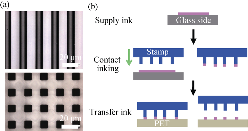
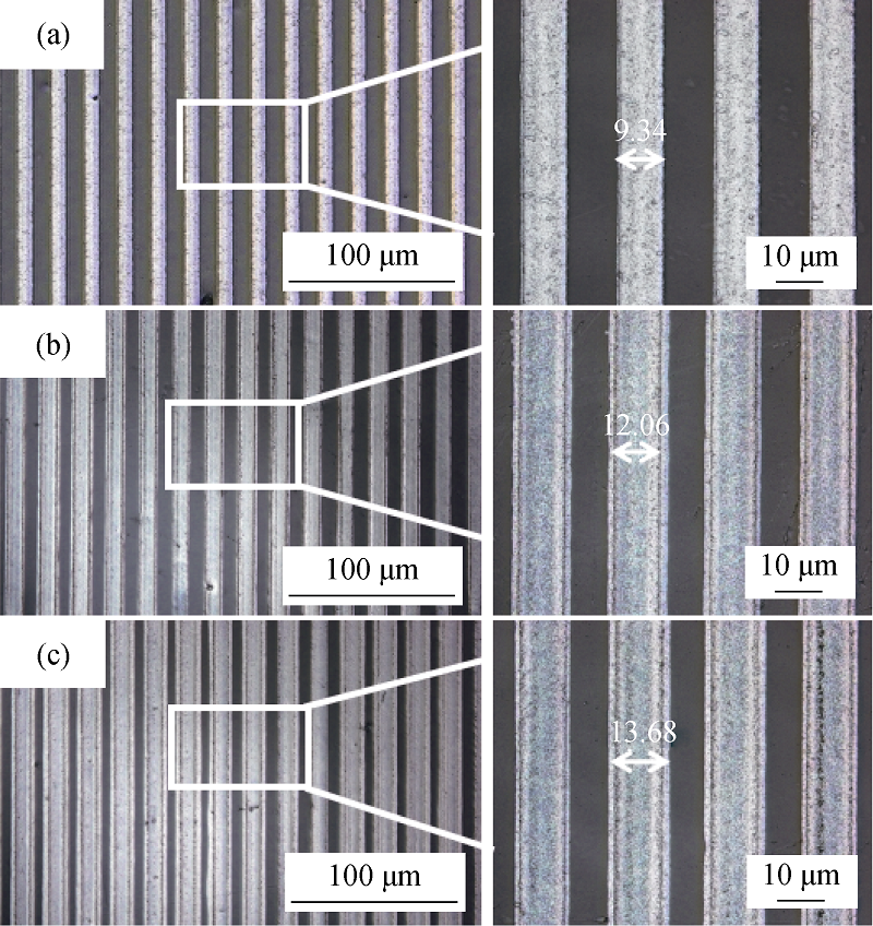
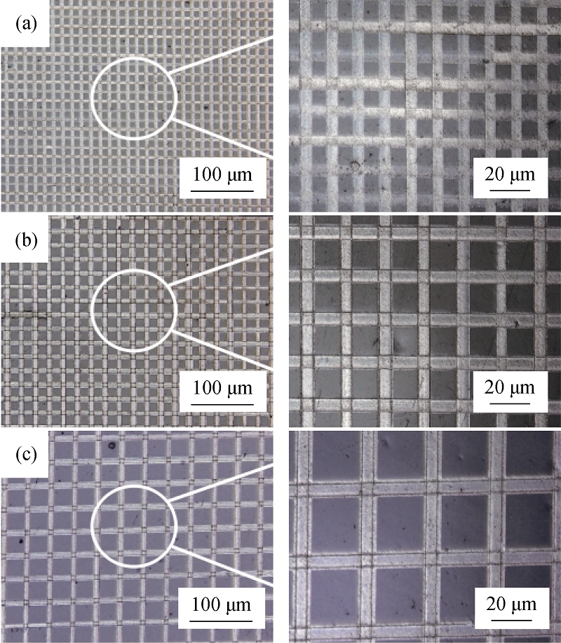
| [1] |
ZHOU L S, WANGA A, WU S C, et al. All-organic active matrix flexible display. Appl. Phys. Lett., 2006, 88(8): 083502-1-3.
|
| [2] |
VUORINEN T, ZAKRZEWSKI M, RAJALA S, et al.Printable, transparent, and flexible touch panels working in sunlight and moist environments. Adv. Funct. Mater., 2014, 24(40): 6340-6347.
|
| [3] |
LIPOMI D J, TEE B C K, VOSGUERITCHIAN M. et al. Stretchable organic solar cells.Adv. Mater., 2011, 23(15): 1771-1775.
|
| [4] |
TOKUNO T, NOGI M, KARAKAWA M, et al.Fabrication of silver nanowire transparent electrodes at room temperature.Nano Res., 2011, 4(12): 1215-1222.
|
| [5] |
LAYANI M, GRUCHKO M, MILO O, et al.Transparent conductive coatings by printing coffee ring arrays obtained at room temperature.ACS Nano, 2009, 3(11): 3537-3542.
|
| [6] |
KIM Y, NA J, PARK C, et al.PEDOT as a flexible organic electrode for a thin film acoustic energy harvester. ACS Appl. Mater. Inter., 2015, 7(30): 16279-16286.
|
| [7] |
WU Q, XU Y, YAO Z, et al.Supercapacitors based on flexible graphene/polyaniline nanofiber composite films.ACS Nano, 2010, 4(4): 1963-1970.
|
| [8] |
DEGANELLO D, CHERRY J A, GETHIN D T, et al.Patterning of micro-scale conductive networks using reel-to-reel flexographic printing.Thin Solid Films, 2010, 518(21): 6113-6116.
|
| [9] |
PARK J, NGUYEN H A D, PARK S, et al. Roll-to-roll gravure printed silver patterns to guarantee printability and functionality for mass production.Current Applied Physics, 2015, 15(3): 367-376.
|
| [10] |
OH S C, YANG K Y, BYEON K J, et al.Various metallic nano-sized patterns fabricated using an Ag ink printing technique.Electron Mater. Lett., 2012, 8(5): 485-489.
|
| [11] |
KUMAR A, BIEBUYCK H A, WHITESIDES G M.Patterning self-assembled monolayers: applications in materials science.Langmuir, 1994, 10(5): 1498-1511.
|
| [12] |
YAN X, YAO J, LU G, et al.Microcontact printing of colloidal crystals.J. Am. Chem. Soc., 2004, 126(34): 10510-10511.
|
| [13] |
KIM L, ANIKEEVA P O, COE-SULLIVAN S A, et al. Contact printing of quantum dot light-emitting devices.Nano Lett., 2008, 8(12): 4513-4517.
|
| [14] |
HIDBER P C, HELBIG W, KIM E, et al.Microcontact printing of palladium colloids: micron-scale patterning by electroless deposition of copper.Langmuir, 1996, 12(5): 1375-1380.
|
| [15] |
TANG J, PANG W H, REN H, et al.Rapid transfer of Au nanoparticle pattern onto ITO substrate using microcontact printing technique.Acta Phys. - Chim. Sin., 2013, 29(3): 612-618.
|
| [16] |
KUSAKA Y, MIYASHITA K, USHIJIMA H. Extending microcontact printing for patterning of thick polymer layers: semi-drying of inks and contact mechanisms. J. Micromech. Microeng., 2014, 24(12): 125019-1-10.
|
| [17] |
KINA O, KOUTAKE M, MATSUOKA K, et al. Organic thin-film transistors fabricated by microcontact printing. Jpn. J. Appl. Phys., 2010, 49(1):01AB07-1-4.
|
| [18] |
KUSAKA Y, NOMURA K, FUKUDA N, et al. Microcontact patterning of conductive silver lines by contact inking and its layer- transfer mechanisms. J. Micromech. Microeng., 2015, 25(5): 055022-1-9.
|
| [19] |
LIU S, XIN Z, LI X, et al.Conductive microwires of silver nanoparticles prepared by microcontact printing.J. Nano. Res., 2016, 37(1): 36-41.
|
| [20] |
ZHANG Z, ZHANG X, XIN Z, et al. Synthesis of monodisperse silver nanoparticles for ink-jet printed flexible electronics. Nanotechnology, 2011, 22(42): 425601-1-8.
|
| [21] |
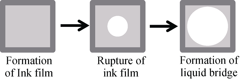
XIN Z, SU B, WANG J, et al.Continuous microwire patterns dominated by controllable rupture of liquid films.Small, 2013, 9(5): 722-726.
|