无机材料学报 ›› 2014, Vol. 29 ›› Issue (12): 1233-1240.DOI: 10.15541/jim20140110
• • 下一篇
朱信华1, 李爱东2, 刘治国2
收稿日期:2014-03-10
修回日期:2014-04-15
出版日期:2014-12-20
网络出版日期:2014-11-20
基金资助:ZHU Xin-Hua1, LI Ai-Dong2, LIU Zhi-Guo2
Received:2014-03-10
Revised:2014-04-15
Published:2014-12-20
Online:2014-11-20
Supported by:摘要:
扫描透射电子显微镜(STEM)原子序数衬度像(Z-衬度像)具有分辨率高(可直接“观察”到晶体中原子的真实位置)、对化学组成敏感以及图像直观易解释等优点, 成为原子尺度研究材料微结构的强有力工具。本文介绍了STEM Z-衬度像成像原理、方法及技术特点, 并结合具体的高K栅介质材料 (如铪基金属氧化物、稀土金属氧化物和钙钛矿结构外延氧化物薄膜)对STEM在新一代高K栅介质材料研究中的应用进行了评述。 目前球差校正STEM Z-衬度的像空间分辨率已达亚埃级, 该技术在高K柵介质与半导体之间的界面微结构表征方面具有十分重要的应用。对此, 本文亦进行了介绍。
中图分类号:
朱信华, 李爱东, 刘治国. 扫描透射电子显微镜(STEM)在新一代高K栅介质材料的应用[J]. 无机材料学报, 2014, 29(12): 1233-1240.
ZHU Xin-Hua, LI Ai-Dong, LIU Zhi-Guo. Applications of Scanning Transmission Electron Microscopy (STEM) in the New Generation of High-K Gate Dielectrics[J]. Journal of Inorganic Materials, 2014, 29(12): 1233-1240.
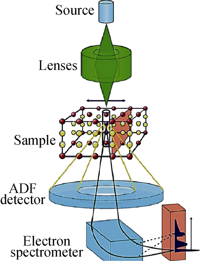
图1 扫描透射电子显微像(STEM)形成示意图[6]
Fig. 1 Schematic diagram for the formation of STEM image[6]
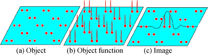
图2 (a)样品的原子柱二维投影(Si〈110〉方向)、(b)样品高角散射时的钉状物体势函数和(c)实验像强度分布解释为物体的势函数与电子束斑强度函数的卷积[8]
Fig. 2 Potential for high-angle scattering of Si atomic columms The specimen in (a) consists of an array of atomic columns (〈110〉 Si for example), in which the potential for high-angle scattering can be represented by an object function consisting of weighted spikes, as shown in (b). The experimental image can be interpreted as a convolution of the experimental probe and the object function, as in (c)[8]
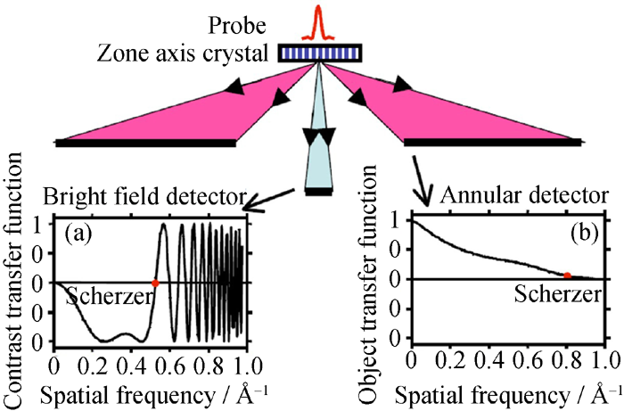
图3 扫描透射电子显微镜(VG Microscopes HB501UX STEM 工作电压100 kV, 电子束斑尺寸 ~ 0.22 nm)在(a)相干和(b)非相干成像条件下的不同衬度传递函数 [6]
Fig. 3 Different contrast transfer functions of a STEM (VG Microscopes HB501UX STEM operated at 100 kV with a probe size of ~ 0.22 nm) measured simultaneously at (a) coherent and (b) incoherent imaging conditions by using a small bright field detector and a large annular detector, respectively Plots show the very different transfer functions for the two detectors, the bright field detector showing contrast reversals and oscillations characteristic of coherent phase contrast imaging, the dark field detector showing a monotonic decrease in transfer with spatial frequency characteristic of incoherent imaging[6]
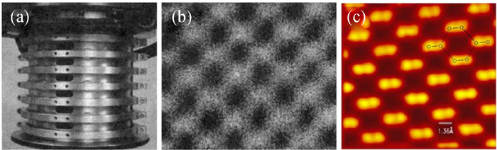
图4 球差校正器及其对Z-STEM像分辨率的改善[11]
Fig. 4 Aberration corrector and improvement of Z-STEM image resolution [11] (a) An Aberration corrector consisting of 60 optical components, (b) experimental Z-STEM image of Si in [110] orientation taken from VG STEM HB501 STEM with a point resolution of ~ 0.2 nm, un-resolving the dumbbell structure of silicon, and (c) Z-STEM image of Si in [110] orientation taken from VG STEM HB501 STEM equipped with Nion aberration corrector, resolving clearly the dumbbell unit structure of silicon with a point resolution of 0.13 nm and increasing the ratio of signal-to-noise
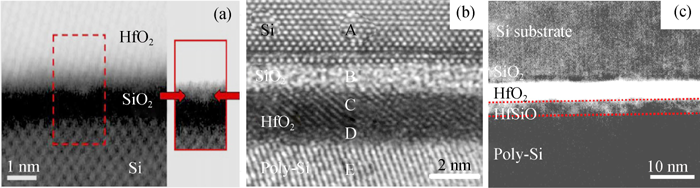
图5 (a) Si/HfO2堆垛结构的剖面Z-STEM像, HfO2/SiO2的界面结构见图的中心部分[16], (b)沿Si衬底[110]方向观察HfO2/HfSiO堆垛结构的剖面HRETM像和(c)相同堆垛结构的剖面Z-STEM像[17]
Fig. 5 Images of Si/HfO2 (a) and HfO2/HfSiO (b,c) gate stacks (a) Cross-sectional Z-STEM image of an Si/HfO2 gate stack. The SiO2/HfO2 interface is seen in the center of the image[16]; (b) Cross-sectional HRTEM image of a HfO2/HfSiO gate stack viewed from the [110] direction of Si substrate, and (c) HAADF image of the same stack[17]
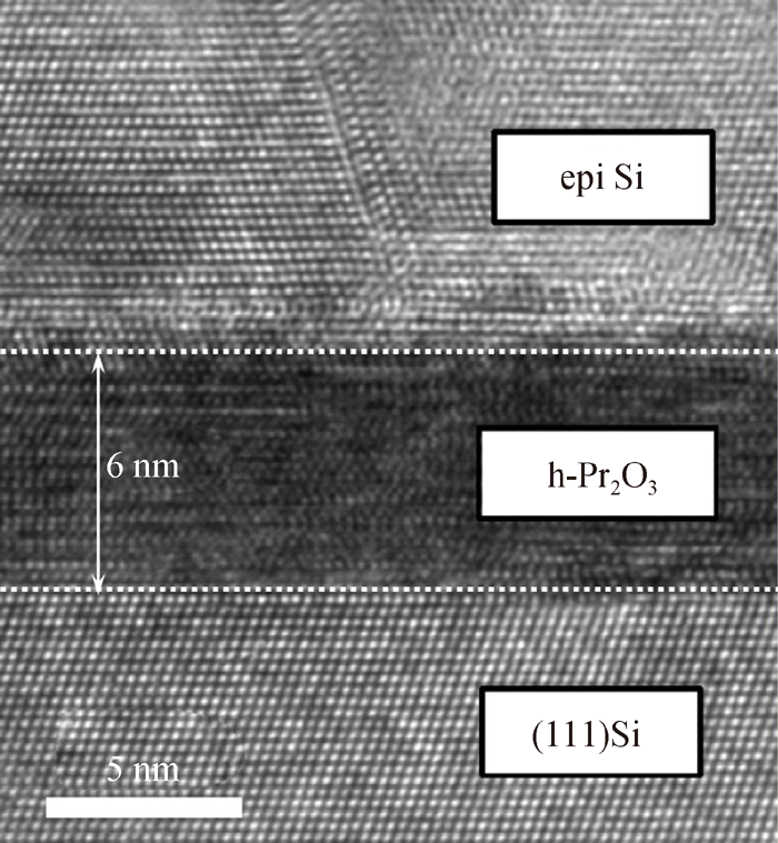
图6 Si(111)衬底上外延生长的Pr2O3薄膜剖面HRTEM像,在Pr2O3薄膜上又外延生长Si (111)薄膜[20]
Fig. 6 Cross-sectional HRTEM image of the epitaxial Pr2O3 film (6 nm thick) grown on Si(111) substrate, and the film can be overgrown epitaxially with high quality Si (111) film[20]
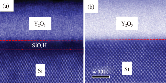
图7 (a) a-Si/Y2O3/c-Si(单晶硅)堆垛结构的Z-STEM像。由于Y2O3薄膜暴露到在大气中, 在Y2O3/c-Si衬底的界面处形成SiOxHy界面反应层, 如图中虚线标注所示; (b) 相同堆垛结构的剖面Z-STEM像, 但Y2O3薄膜在沉积过程中原位覆盖一层非晶硅层(a-Si), 在Y2O3/Si界面处就观察不到SiOxHy反应层[21]
Fig. 7 Z-STEM image of a-Si/Y2O3/c-Si stack (a) The formation of SiOxHy interfacial layer was due to the exposure of Y2O3 film to atmospheric conditions; (b) The interfacial layer of SiOxHy was not visible due to the Y2O3 film in-situ capped by a layer of amorphous Si during the deposited process[21]
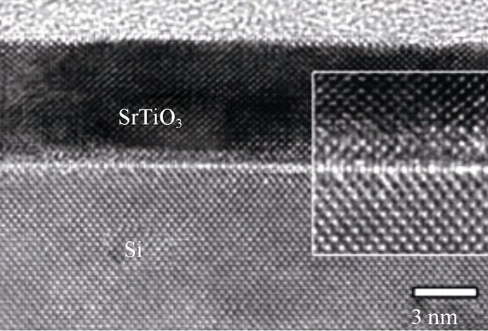
图8 Si(001)衬底上分子束外延生长的SrTiO3薄膜剖面HRTEM像, 显示在SrTiO3薄膜和Si衬底之间形成原子级锐变的界面[23]
Fig. 8 Cross-sectional HRTEM image of a SrTiO3 film epitaxially grown on Si (100) substrate by MBE, showing the formation of an atomically abrupt crystalline interface between the SrTiO3 and Si[23]
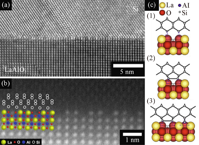
图 9 (a)外延Si/LaAlO3界面的HRTEM像, (b) HAADF-STEM像, 该图像表明界面具有一个3 × 1 的界面重构(即每3个La原子中间就有一个La原子在界面处消失)和(c)基于界面结构的Z-STEM像构筑的Si/LaAlO3界面结构模型[25]
Fig. 9 (a) HRTEM and (b) HAADF-STEM images from an epitaxial Si/LaAlO3 interface showing an interface reconstruction where every third La column is missing at the interface. (c) Interface models based on the HAADF-STEM images[25]
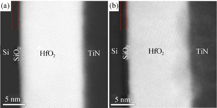
图10 不同退火温度下,原子层沉积(ALD)法生长的HfO2薄膜与TiN金属栅电极及Si衬底之间的界面结构的Z-STEM像[26]
Fig. 10 Z-STEM images of the HfO2 gate dielectrics grown by atomic layer deposition on Si substrates and their interfaces with TiN electrodes and silicon, annealed at (a) 800℃ and (b) 900℃[26] The dashed lines are a guide to the eye to indicate the approximate position of the interfacial layer. Note the roughening of interfaces after annealing at 900℃
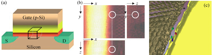
图11 Hf 原子在Si/SiO2/HfO2 堆垛器件中的三维分布[30]
Fig. 11 Three-dimensional locations of single Hf atoms in a Si/SiO2/HfO2 stacked device[30] (a) A schematic view diagram of the Si/SiO2/HfO2 stacked device with a SiO2 layer shown in red and the alternative dielectric, HfO2 shown in yellow color, where S and D representing the source and drain, respectively. (b) Three ADF images of the stack is represented by slice views in planes of x-y, x-z, and y-z, respectively. One isolated single Hf atom is marked the white circles. This representation demonstrates that the Hf atom is located inside the TEM sample. (c) A 3D reconstruction of part of the HfO2/SiO2/Si interface structure showing single Hf atoms. The Si substrate was color coded in gold, whereas the HfO2 film is marked solid yellow. Single Hf atoms with different positions within the interface layer are coded separately in green, black, red, and blue colors, respectively
| [1] | LI D X.High-resolution transmission electron microscopy in materials science-developed history, current status and prospect. J. Chin. Electr. Microscopy Soc., 2000, 19(2): 81-83. |
| [2] | VARELA M, LUPINI A R, BENTHEM K V, et al.Materials characterization in the aberration-corrected scanning transmission electron microscope. Annu. Rev. Mater. Res., 2005, 35: 539-569. |
| [3] | WILK G D, WALLACE R M, ANTHONY J M.High-k gate dielectrics: current status and materials properties considerations. J. Appl. Phys., 2001, 89(10): 5243-5275. |
| [4] | ZHU X H, ZHU J M, LI A D, et al.Challenges in atomic-scale characterization of high-k dielectrics and metal gate electrodes for advanced CMOS gate stacks. J. Mater. Sci. Technol., 2009, 25(3): 289-313. |
| [5] | DELLBY N, KIRVANEK O L, NELLIST P D, et al.Progress in aberration-corrected scanning transmission electron microscopy. J. Electron Microscopy, 2001, 50(3): 177-185. |
| [6] | PENNUCOOK S J.Structure determination through Z-contrast microscopy. Advances in Imaging and Electron Physics, 2002, 123: 173-206. |
| [7] | PENNUCOOK S J, BOATNER L A.Chemically sensitive structure- imaging with a scanning transmission electron microscope. Nature, 1988, 336: 565-567. |
| [8] | BROWNING N D, WALLIS D J, NELLIST P D.EELS in the STEM: determination of materials properties on the atomic scale. Micron, 1997, 28(5): 333-348. |
| [9] | BROWNING N D, BUBAN J P, PROUTEAU C, et al.Investigating the atomic scale structure and chemistry of grain boundaries in High-Tc superconductors. Micron, 1999, 30(3): 425-436. |
| [10] | PENNUCOOK S J, JESSON D E.High-resolution Z-contrast imaging of crystals. Ultramicroscopy, 1991, 37(124):14-38. |
| [11] | PENNUCOOK S J, RAFFERTY B, NELLIST P D.Z-contrast imaging in and aberration-corrected scanning transmission electr on microscope. Microscopy and Microanalysis, 2000, 6: 343-352. |
| [12] | BUCHANAN D.Scaling the gate dielectric: materials, integration, and reliability. IBM J. Res. & Dev., 1999, 43(3): 245-264. |
| [13] | BERSUKER G, ZEITZOFF P, BROWN G, et al.Dielectrics for future transistors. Material Today, 2004, 7(1): 26-33. |
| [14] | ROBERSON J.High dielectric constant gate oxides for metal oxide Si transistors. Rep. Prog. Phys., 2006, 69(2): 327-396. |
| [15] | ZHU X H, ZHU J M, LIU Z G, et al.Characterization of high-K gate dielectrics by atomic-resolution electron microscopy: current progress and future prospects. J. Chin. Electr. Microscopy Soc.,2009, 28(3): 280-302. |
| [16] | GARFUNKELD E, GUSTAFSSON T, LYSAGHT P, et al.Structure, composition and order at interfaces of crystalline oxides and other high-K materials on silicon. FUTURE FAB Inter, 2006, 220: 349-360 |
| [17] | CRAVEN A J, MACKENZIE M, MCCOMB D W, et al. Investigating physical and chemical changes in high-K gate stacks using nanoanalytical electron microscopy. Microelectron Eng., 2005, 80: 90-97. |
| [18] | OSTEN H J, LAHA A, CZERNOHORSKY M, et al.Introducing crystalline rare-earth oxides into Si technologies. Phys. Stat. Sol.(a), 2008, 205(4): 695-707 . |
| [19] | LAHA A, FISSEL A, BUGIEL E, et al.Epitaxial multi-component rare earth oxide for high-K application. Thin Solid Films, 2007, 515(16): 6512-6517. |
| [20] | OSTEN H J, CZERNOHORSKY M, DARGIS R, et al.Integration of functional epitaxial oxides into silicon: from high-K application to nanostructures. Microelectron Eng., 2007, 84(9/10): 2222-2225. |
| [21] | BUSCH B W, PLUCHERY O, CHABAL Y J, et al.Materials characterization of alternative gate dielectrics. MRS Bull., 2002, 27(3): 206-211. |
| [22] | SCHLOM D G, HAENI J H.A thermodynamic approach to selecting alternative gate dielectrics. MRS Bull., 2002, 27(3): 198-204 . |
| [23] | MARCHIORI C, SOUSA M, GUILLER A, et al. Thermal stability of the SrTiO3/(Ba,Sr)O3 stacks epitaxially grown on Si. Appl. Phys. Lett., 2006, 88(7): 072913-1-3. |
| [24] | NORGA G J, MARCHIORI C, ROSSEL C, et al. Solid phase epitaxy of SrTiO3 on (Ba,Sr)O/Si(100): the relationship between oxygen stoichiometry and interface stability. J. Appl. Phys., 2006, 99(8): 84102-1-7. |
| [25] | KLENOV D O, SCHLOM D G, Li H, et al. The interface between single crystalline (001) LaAlO3 and (001) silicon. Jpn. J. Appl. Phys., 2005, 44(20-23): L617-L619. |
| [26] | AGUSTIN M P, FONSECA L R C, HOOKER J C, et al. Scanning transmission electron microscopy of gate stacks with HfO2 dielectrics and TiN electrodes. Appl. Phys. Lett., 2005, 87(12): 121909-1-3. |
| [27] | CHOI K, ALSHAREEF H N, WEN H C, et al. Effective work function modification of atomic-layer-deposited-TaN film by capping layer. Appl. Phys. Lett., 2006, 89(3): 032113-1-3. |
| [28] | ANDERSON S C, BIRKELAND C R, ANSTIS G R, et al.An approach to quantitative compositional profiling at near-atomic resolution using high-angle annular dark field imaging. Ultramicroscopy, 1997, 69(2): 83-103. |
| [29] | PENNUCOOK S J, JESSON D E, MCGIBBON A J, et al.High angle dark field STEM for advanced materials. J. Electron Microscopy, 1996, 45(1): 36-43. |
| [30] | BENTHEMA K V, LUPINI A R, KIM M Y, et al. Three-dimensional imaging of individual hafnium atoms inside a semiconductor device. Appl. Phys. Lett., 2005, 87(3): 034104-1-3. |
| [1] | 丁玲, 蒋瑞, 唐子龙, 杨运琼. MXene材料的纳米工程及其作为超级电容器电极材料的研究进展[J]. 无机材料学报, 2023, 38(6): 619-633. |
| [2] | 杨卓, 卢勇, 赵庆, 陈军. X射线衍射Rietveld精修及其在锂离子电池正极材料中的应用[J]. 无机材料学报, 2023, 38(6): 589-605. |
| [3] | 陈强, 白书欣, 叶益聪. 热管理用高导热碳化硅陶瓷基复合材料研究进展[J]. 无机材料学报, 2023, 38(6): 634-646. |
| [4] | 林俊良, 王占杰. 铁电超晶格的研究进展[J]. 无机材料学报, 2023, 38(6): 606-618. |
| [5] | 牛嘉雪, 孙思, 柳鹏飞, 张晓东, 穆晓宇. 铜基纳米酶的特性及其生物医学应用[J]. 无机材料学报, 2023, 38(5): 489-502. |
| [6] | 苑景坤, 熊书锋, 陈张伟. 聚合物前驱体转化陶瓷增材制造技术研究趋势与挑战[J]. 无机材料学报, 2023, 38(5): 477-488. |
| [7] | 杜剑宇, 葛琛. 光电人工突触研究进展[J]. 无机材料学报, 2023, 38(4): 378-386. |
| [8] | 杨洋, 崔航源, 祝影, 万昌锦, 万青. 柔性神经形态晶体管研究进展[J]. 无机材料学报, 2023, 38(4): 367-377. |
| [9] | 游钧淇, 李策, 杨栋梁, 孙林锋. 氧化物双介质层忆阻器的设计及应用[J]. 无机材料学报, 2023, 38(4): 387-398. |
| [10] | 陈昆峰, 胡乾宇, 刘锋, 薛冬峰. 多尺度晶体材料的原位表征技术与计算模拟研究进展[J]. 无机材料学报, 2023, 38(3): 256-269. |
| [11] | 张超逸, 唐慧丽, 李宪珂, 王庆国, 罗平, 吴锋, 张晨波, 薛艳艳, 徐军, 韩建峰, 逯占文. 新型GaN与ZnO衬底ScAlMgO4晶体的研究进展[J]. 无机材料学报, 2023, 38(3): 228-242. |
| [12] | 齐占国, 刘磊, 王守志, 王国栋, 俞娇仙, 王忠新, 段秀兰, 徐现刚, 张雷. GaN单晶的HVPE生长与掺杂进展[J]. 无机材料学报, 2023, 38(3): 243-255. |
| [13] | 林思琪, 李艾燃, 付晨光, 李荣斌, 金敏. Zintl相Mg3X2(X=Sb, Bi)基晶体生长及热电性能研究进展[J]. 无机材料学报, 2023, 38(3): 270-279. |
| [14] | 刘岩, 张珂颖, 李天宇, 周菠, 刘学建, 黄政仁. 陶瓷材料电场辅助连接技术研究现状及发展趋势[J]. 无机材料学报, 2023, 38(2): 113-124. |
| [15] | 谢兵, 蔡金峡, 王铜铜, 刘智勇, 姜胜林, 张海波. 高储能密度聚合物基多层复合电介质的研究进展[J]. 无机材料学报, 2023, 38(2): 137-147. |
| 阅读次数 | ||||||
|
全文 |
|
|||||
|
摘要 |
|
|||||