Journal of Inorganic Materials ›› 2016, Vol. 31 ›› Issue (4): 358-364.DOI: 10.15541/jim20150455
• Orginal Article • Previous Articles Next Articles
LIU Chang1, YUAN Shuai2, ZHANG Hai-Liang2, CAO Bing-Qiang2, WU Li-Li1, YIN Long-Wei1
Received:2015-09-28
Revised:2015-11-21
Published:2016-04-20
Online:2016-03-25
About author:LIU Chang. E-mail: liuchangsdu@foxmail.com
Supported by:CLC Number:
LIU Chang, YUAN Shuai, ZHANG Hai-Liang, CAO Bing-Qiang, WU Li-Li, YIN Long-Wei. p-type CuI Films Grown by Iodination of Copper and Their Application As Hole Transporting Layers for Inverted Perovskite Solar Cells[J]. Journal of Inorganic Materials, 2016, 31(4): 358-364.
| Sample No. | Reaction time/ min | Reaction temperature/℃ | Cu/I ratio |
|---|---|---|---|
| 1 | 15 | 120 | 1:1 |
| 2 | 30 | 120 | 1:1 |
| 3 | 45 | 120 | 1:1 |
| 4 | 60 | 120 | 1:1 |
| 5 | 30 | 120 | 1:1 |
| 6 | 30 | 140 | 1:1 |
| 7 | 30 | 160 | 1:1 |
| 8 | 30 | 180 | 1:1 |
| 9 | 30 | 140 | 1:1 |
| 10 | 30 | 140 | 1:10 |
| 11 | 30 | 140 | 1:100 |
Table 1 Growth condition of iodination of copper film
| Sample No. | Reaction time/ min | Reaction temperature/℃ | Cu/I ratio |
|---|---|---|---|
| 1 | 15 | 120 | 1:1 |
| 2 | 30 | 120 | 1:1 |
| 3 | 45 | 120 | 1:1 |
| 4 | 60 | 120 | 1:1 |
| 5 | 30 | 120 | 1:1 |
| 6 | 30 | 140 | 1:1 |
| 7 | 30 | 160 | 1:1 |
| 8 | 30 | 180 | 1:1 |
| 9 | 30 | 140 | 1:1 |
| 10 | 30 | 140 | 1:10 |
| 11 | 30 | 140 | 1:100 |

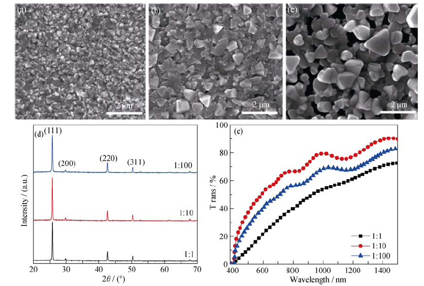
Fig. 2 SEM images of CuI films deposited with different Cu/I ratios and corresponding XRD patterns and optical transmission spectra (a) 1:1, (b) 1:10, (c) 1:100
| Cu/I ratio | Resistivity/(10-2 Ω·cm) | Mobility/(cm2·V-1·s-1) |
|---|---|---|
| 1:1 | 8.9 | 8.6 |
| 1:10 | 8.2 | 13.5 |
| 1:100 | 11.1 | 1.5 |
Table 2 Hall effect data of CuI films grown with different Cu/I ratios
| Cu/I ratio | Resistivity/(10-2 Ω·cm) | Mobility/(cm2·V-1·s-1) |
|---|---|---|
| 1:1 | 8.9 | 8.6 |
| 1:10 | 8.2 | 13.5 |
| 1:100 | 11.1 | 1.5 |

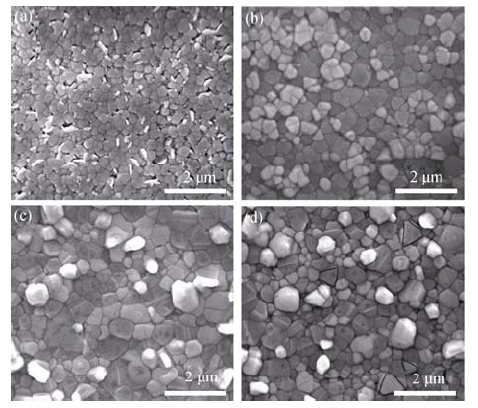
Fig. 3 Surface morphology SEM images of CuI films grown under different iodination temperature and iodination time (a) 15 min, 120℃; (b) 30 min, 120℃; (c) 45 min, 120℃; (d) 30 min, 160℃
| Iodination time/temperature | Resistivity/ (10-2 Ω·cm) | Mobility/ (cm2·V-1·s-1) |
|---|---|---|
| 15 min/120℃(Ⅰ) | 9.9 | 14.9 |
| 30 min/120℃(Ⅱ) | 4.4 | 29.6 |
| 45 min/120℃(Ⅲ) | 7.1 | 17.1 |
| 30 min/160℃(Ⅳ) | 13.9 | 9.5 |
Table 3 Hall effect data of CuI films grown under different iodination temperature and time
| Iodination time/temperature | Resistivity/ (10-2 Ω·cm) | Mobility/ (cm2·V-1·s-1) |
|---|---|---|
| 15 min/120℃(Ⅰ) | 9.9 | 14.9 |
| 30 min/120℃(Ⅱ) | 4.4 | 29.6 |
| 45 min/120℃(Ⅲ) | 7.1 | 17.1 |
| 30 min/160℃(Ⅳ) | 13.9 | 9.5 |

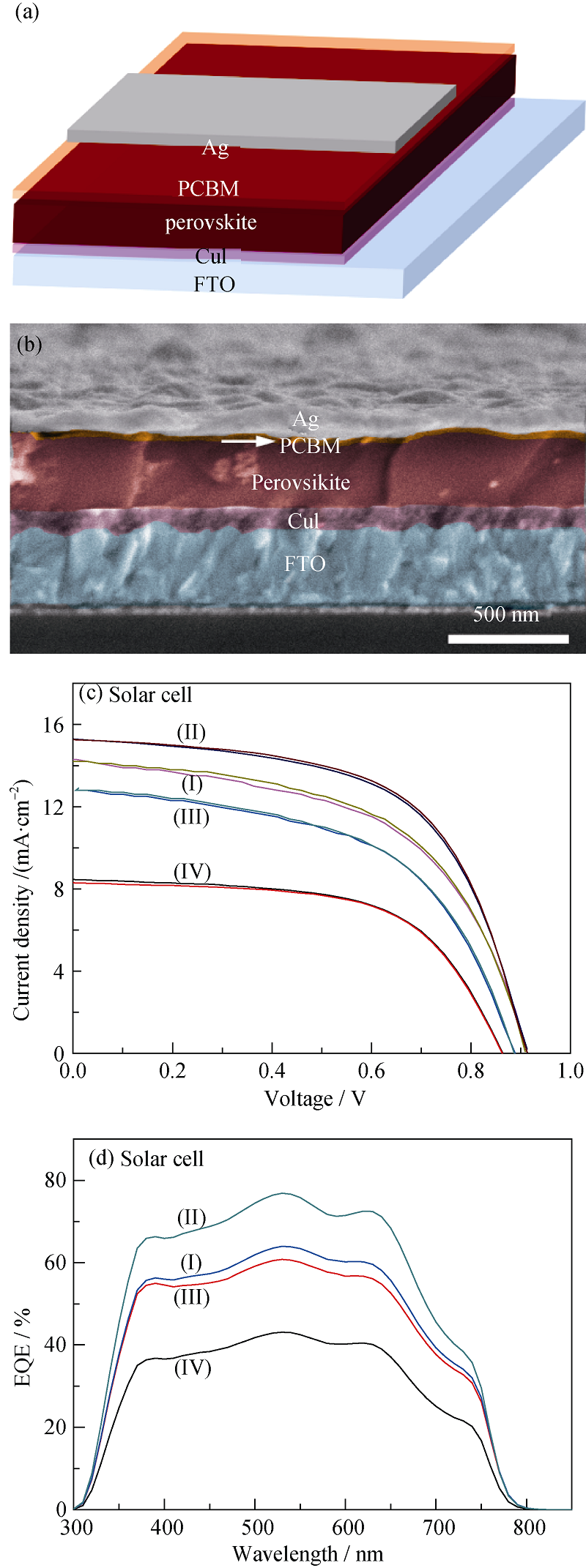
Fig. 5 (a) Schematic diagram and (b) typical SEM image of CuI film based planar perovskite solar cell. (c) Current density-voltage (J-V) characteristic curves and (d) EQE curves of the perovskite solar cells assembled with different CuI films as hole transporting layers. Curves labeled with (I~IV) correspond to samples (I~IV) in Table 3 grown under different iodination temperature and time
| Devices | VOC/V | JSC/(mA·cm-2) | FF/% | η /% |
|---|---|---|---|---|
| I | 0.92 | 14.26 | 53.73 | 7.05 |
| II | 0.93 | 15.33 | 58.51 | 8.35 |
| III | 0.89 | 12.84 | 54.01 | 6.17 |
| IV | 0.86 | 8.45 | 51.70 | 3.75 |
Table 4 Corresponding photovoltaic properties of perovskite solar cells (I-IV) with different CuI as hole transporting layer
| Devices | VOC/V | JSC/(mA·cm-2) | FF/% | η /% |
|---|---|---|---|---|
| I | 0.92 | 14.26 | 53.73 | 7.05 |
| II | 0.93 | 15.33 | 58.51 | 8.35 |
| III | 0.89 | 12.84 | 54.01 | 6.17 |
| IV | 0.86 | 8.45 | 51.70 | 3.75 |
| [1] | BÜHERE W, HÄLG W. Crystal structure of high-temperature cuprous iodide and cuprous bromide.International Symposium on Solid Ionic and Ionic-Electronic Conductors, 1977, 22(7): 701-704. |
| [2] | MIYAKE S, HOSHINO S, TAKENAKA T.On the phase transition in cuprous iodide.Journal of the Physics Society of Japan, 1952, 7(1): 19-24. |
| [3] | BOUHAFS B, HEIRECHE H, SEKKAL W, et al.Electronic and optical properties of copper halides mixed crystal CuCl1-xIx.Physics Letters A, 1998, 240(4/5): 257-264. |
| [4] | BÄDEKER K. Über eine eigentümliche Form elektrischen Leitvermögens bei festen Körpern.Annalen der Physik, 1909, 334(8): 566-584. |
| [5] | SCHEIN F L, VON WENCKSTERN H, GRUNDMANN M. Transparent p-CuI/n-ZnO heterojunction diodes. Applied Physics Letters, 2013, 102(9): 092109-1-4. |
| [6] | ZHU B L, ZHAO X Z.Transparent conductive CuI thin films prepared by pulsed laser deposition.Phys. Status Solidi A, 2011, 208(1): 91-96. |
| [7] | ZI M, LI J, ZHANG Z C, et al.Effect of deposition temperature on transparent conductive properties of γ-CuI film prepared by vacuum thermal evaporation.Phys. Status Solidi A, 2015, 212(7): 1466-1470. |
| [8] | WANG H G, BAI X, WEI J Q, et al.Preparation of CuI particles and their applications in carbon nanotube-Si heterojunction solar cells.Materials Letters, 2012, 79:106-108. |
| [9] | KUMARA G R A, TISKUMARA J K, RANASINGHE C S K, et al. Efficient solid-state dye-sensitized n-ZnO/D-358 dye/p-CuI solar cell.Electrochimica Acta, 2013, 94: 34-37. |
| [10] | DAS S, CHOI J Y, ALFORD T L.P3HT:PC61BM based solar cells employing solution processed copper iodide as the hole transport layer.Solar Energy Materials & Solar Cells, 2015, 133: 255-259. |
| [11] | WANG YAN-XIANG, LUO JUN, GUO PING-CHUN, et al.Application and development of hybrid perovskite materials in the field of solar cells.Journal of Inorganic Materials, 2015, 30(7): 673-682. |
| [12] | YANG YING, GAO JING, CUI JIA-RUI, et al.Research progress of perovskite solar cell.Journal of Inorganic Materials, 2015, 30(11): 1131-1138. |
| [13] | YAACOBI-GROSS N, TREAT NEIL D, PATTANASATTAYAVONG P, et al. High-efficiency organic photovoltaic cells based on the solution-processable hole transporting interlayer copper thiocyanate (CuSCN) as a Replacement for PEDOT: PSS. Advanced Energy Materials, 2015, 5(3): 1401529-1-7. |
| [14] | CHRISTIANS J A, FUNG R C M, KAMAT P V. An inorganic hole conductor for organo-lead halide perovskite solar cells. improved hole conductivity with copper iodide.Journal of American Chemical Society, 2014, 136(2): 758-764. |
| [15] | SNAITH H J, ABATE A, BALL J M, et al.Anomalous hysteresis in perovskite solar cells.Journal of Physical Chemistry Letters, 2014, 5: 1511-1515. |
| [16] | CHAVHAN S, MIGUEL O, GRANDE H J, et al.Organo-metal halide perovskite-based solar cells with CuSCN as the inorganic hole selective contact.Journal of Materials Chemistry A, 2014, 2(32): 12754-12760. |
| [17] | STRANKS S D, EPERON G E, GRANCINI G, et al. Electron- hole diffusion lengths exceeding 1 micrometer in an organometal trihalide perovskite absorber.Science, 342(6156): 341-344. |
| [18] | KIM H S, PARK N G.Parameters Affecting I-V hysteresis of ch3nh3pbi3 perovskite solar cells: effects of perovskite crystal size and mesoporous tio2 layer.Journal of Physical Chemistry Letter, 2014, 5(17): 2927-2934. |
| [19] | ZHOU H, CHEN Q, LI G, et al.Interface engineering of highly efficient perovskite solar cells.Science, 2014, 345(6196): 542-546. |
| [20] | SHI J J, DONG J, LV S T, et al. Hole-conductor-free perovskite organic lead iodide heterojunction thin-film solar cells: High efficiency and junction property. Applied Physics Letter, 2014, 104(6): 063901-1-4. |
| [1] | YANG Yingkang, SHAO Yiqing, LI Bailiang, LÜ Zhiwei, WANG Lulu, WANG Liangjun, CAO Xun, WU Yuning, HUANG Rong, YANG Chang. Enhanced Band-edge Luminescence of CuI Thin Film by Cl-doping [J]. Journal of Inorganic Materials, 2023, 38(6): 687-692. |
| [2] | ZHOU Bei-Ying, CHEN Dong, LIU Jia-Le, JIANG Wan, LUO Wei, WANG Lian-Jun. Preparation and Property of CuInS2/ZnS Core-shell Quantum Dots in Aqueous Phase [J]. Journal of Inorganic Materials, 2018, 33(3): 279-283. |
| [3] | LI Feng-Rui, GU Mu, HE Hui, CHANG Li-Hua, WEN Wei-Feng, LI Ze-Ren, CHEN Liang, LIU Jin-Liang, OUYANG Xiao-Ping, LIU Xiao-Lin, LIU Bo, HUANG Shi-Ming,NI Chen. Fluorescent Decay Time and Energy Response of γ-CuI Crystal [J]. Journal of Inorganic Materials, 2017, 32(2): 163-168. |
| [4] | HUANG Rong-Tie, ZHENG Ming, SUI Li-Fang, CAI Chuan-Bing, HUANG Fu-Qiang. Synthesis and Physical Properties of Solar Material Cu1-xLixInSe2 [J]. Journal of Inorganic Materials, 2017, 32(1): 101-106. |
| [5] | TIAN Li, ZHANG Xiao-Yong, MAO Qi-Nan, LI Xue-Geng, YU Ping-Rong, WANG Dong. Effect of Vacuum Rapid Annealing Treatment on Performance of CIGS Solar Cells [J]. Journal of Inorganic Materials, 2015, 30(1): 35-40. |
| [6] | XIE Yi-Jun, GUO Yi-Ping, DONG Wen, GUO Bing, LI Hua, LIU He-Zhou. Preparation of La-doped BiFeO3 Thin Film and Its Photovoltaic Properties [J]. Journal of Inorganic Materials, 2013, 28(4): 436-440. |
| [7] | FAN Jun-Qi, ZHOU Zheng-Ji, ZHOU Wen-Hui, WU Si-Xin. Fabrication of CuInS2 Sensitized TiO2 Nanorod Arrays for Photovoltaic Devices [J]. Journal of Inorganic Materials, 2012, 27(1): 49-53. |
| [8] | YAN Chang, LIU Fang-Yang, LAI Yan-Qing, LI Yi, LI Jie, LIU Ye-Xiang. Structure and Electrical Property of CuInS2 Thin Films Deposited by DC Reactive Magnetron Sputtering [J]. Journal of Inorganic Materials, 2011, 26(12): 1287-1292. |
| [9] | WANG Zhuo,LI Yong-Xiang,YANG Qun-Bao. Progress of Novel Inkjet Technique for Inorganic Materials Preparation [J]. Journal of Inorganic Materials, 2009, 24(6): 1090-1096. |
| [10] | WANG Lin-Jim,FANG Zhi-Jun,ZHANG Ming-Long,SHEN Hu-Jiang,XIA Yi-Ben. Dielectric and Thermal Properties of Diamond Film/Alumina Composite [J]. Journal of Inorganic Materials, 2004, 19(4): 902-906. |
| [11] | WANG YOng-Ling,YU Da-Wei,DONG Xian-Lin. An Idea for Development of Intelligent Materials and Devices [J]. Journal of Inorganic Materials, 1999, 14(2): 211-217. |
| [12] | CHEN Hongbing,ZHU Congshan,GAN Fuxi. Preparation and Electroinduced Second Order Nonlinear Optical Properties of CuI Microcrystal Doped Borosilicate Glasses [J]. Journal of Inorganic Materials, 1997, 12(4): 487-493. |
| Viewed | ||||||
|
Full text |
|
|||||
|
Abstract |
|
|||||