Journal of Inorganic Materials ›› 2014, Vol. 29 ›› Issue (11): 1199-1203.DOI: 10.15541/jim20140087
• Orginal Article • Previous Articles Next Articles
LI Xiao-Shuai1, WANG Zeng-Mei1, 2, ZHU Ming-Fang3, WANG Shan-Peng2, TAO Xu-Tang2, LU Jun1, CHEN Xing-Tao1, XU Jia-Le1
Received:2014-02-27
Revised:2014-04-13
Published:2014-11-20
Online:2014-10-24
About author:LI Xiao-Shuai. E-mail: lixsseu@163.com
Supported by:CLC Number:
LI Xiao-Shuai, WANG Zeng-Mei, ZHU Ming-Fang, WANG Shan-Peng, TAO Xu-Tang, LU Jun, CHEN Xing-Tao, XU Jia-Le. Synthesis of Jumbo-size Single Crystalline Bi2Se3 Nanoplates and Nanoribbons by Vapor Transportation[J]. Journal of Inorganic Materials, 2014, 29(11): 1199-1203.
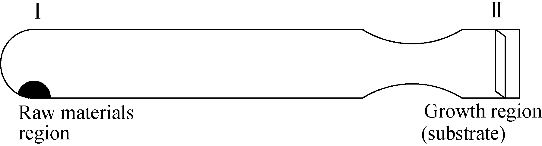
Fig. 1 Schematic of experimental setup for the synthesis of Bi2Se3 nanoplates and nanoribbons with vapor transportation Ⅰ: 700℃; Ⅱ: 350℃-450℃
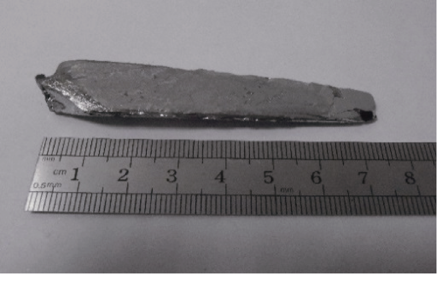
Fig. 2 Bulk Bi2Se3 synthesized by vacuum melting at high temperature
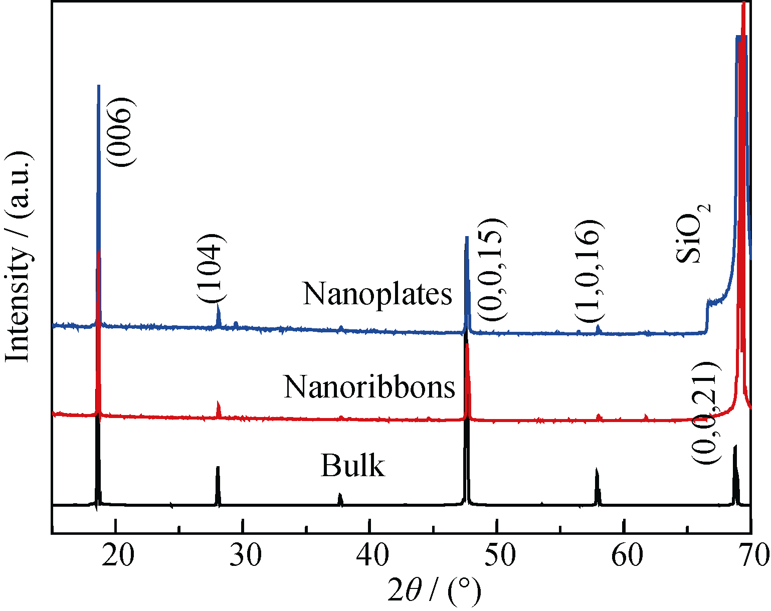
Fig. 3 XRD patterns of bulk Bi2Se3, Bi2Se3 nanoplates and Bi2Se3 nanoribbons
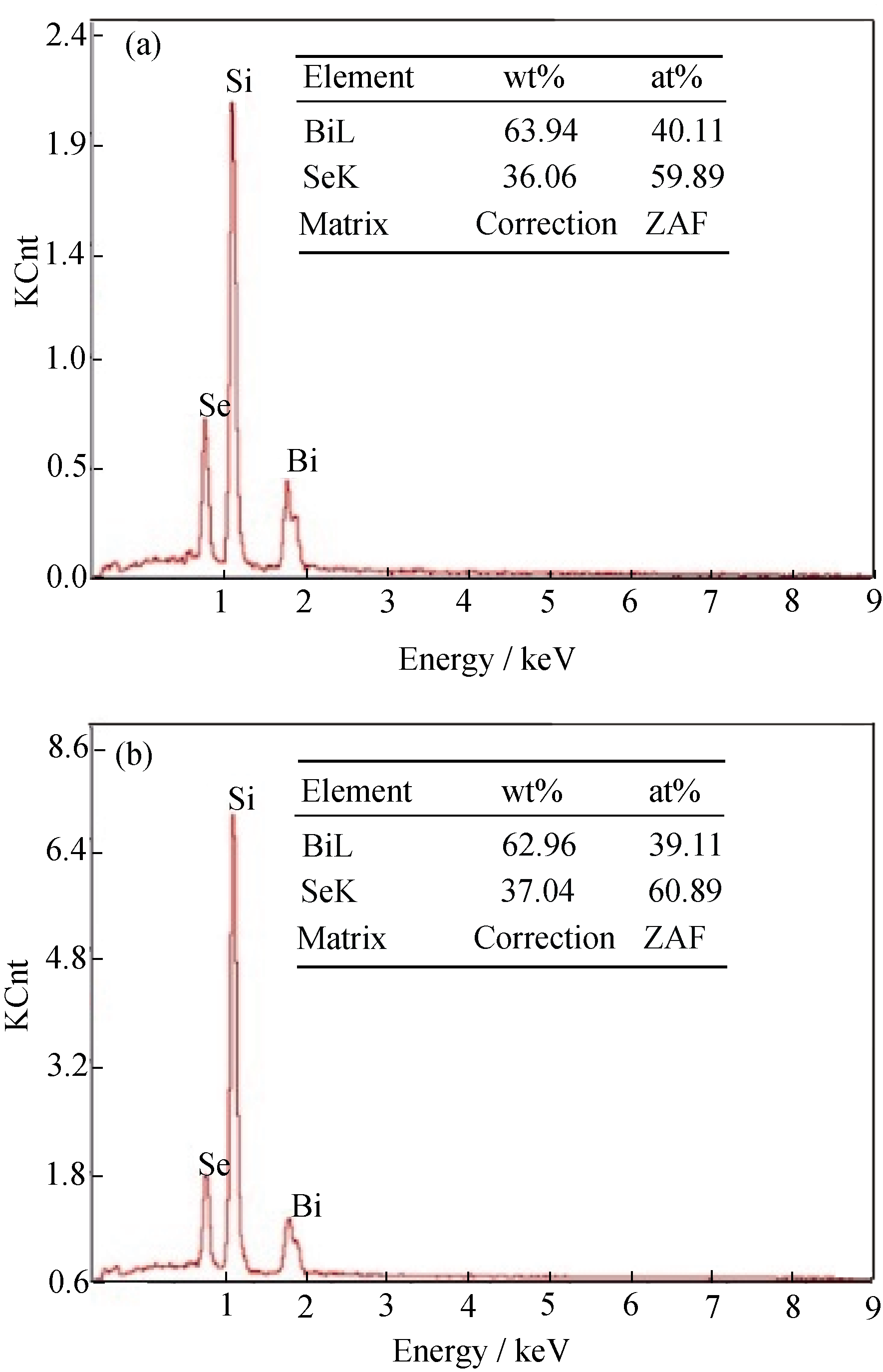
Fig. 4 EDS spectra of Bi2Se3 nanoplates (a) and Bi2Se3 nanoribbons (b)
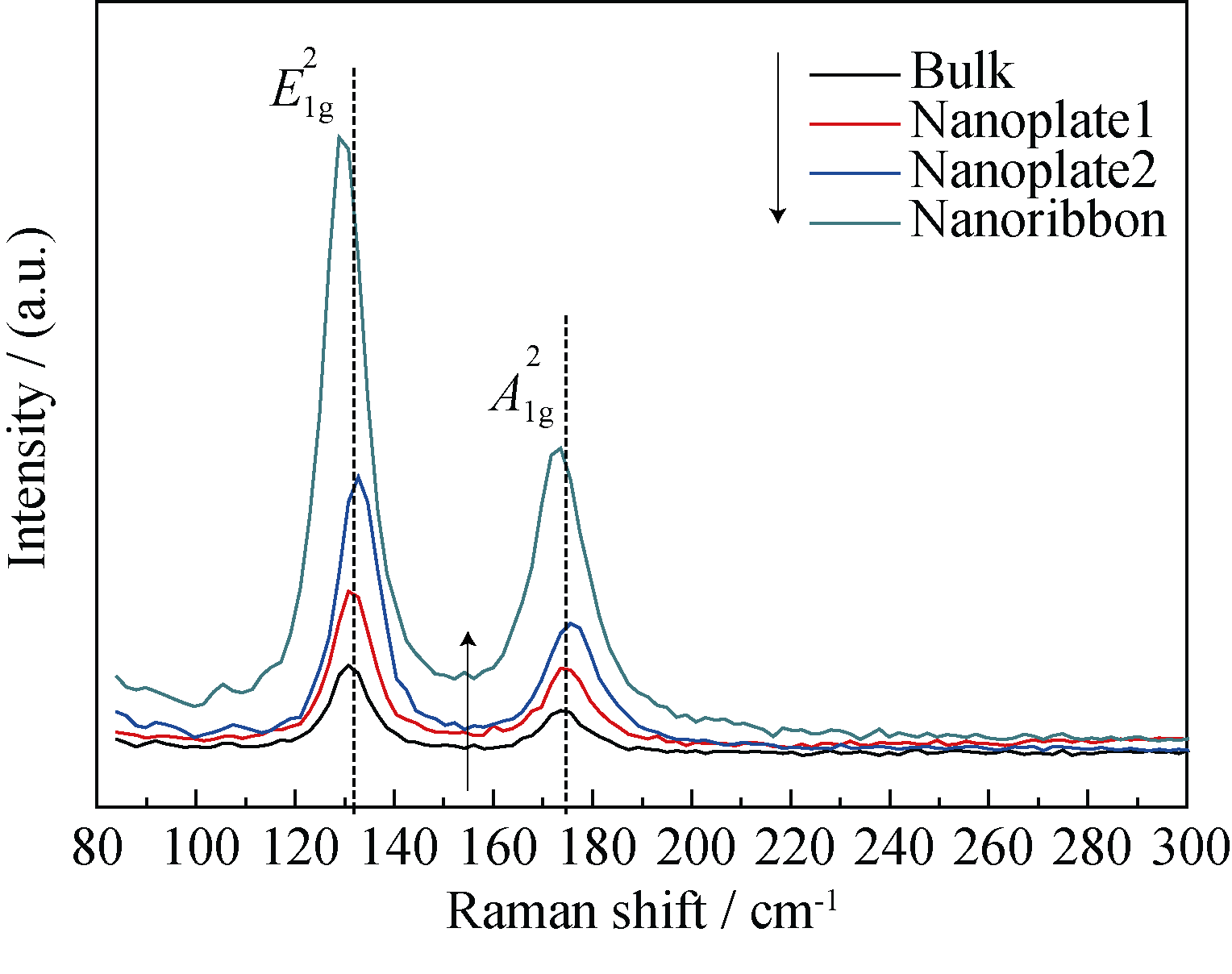
Fig. 5 Raman spectra of bulk Bi2Se3, Bi2Se3 nanoplates and Bi2Se3 nanoribbons
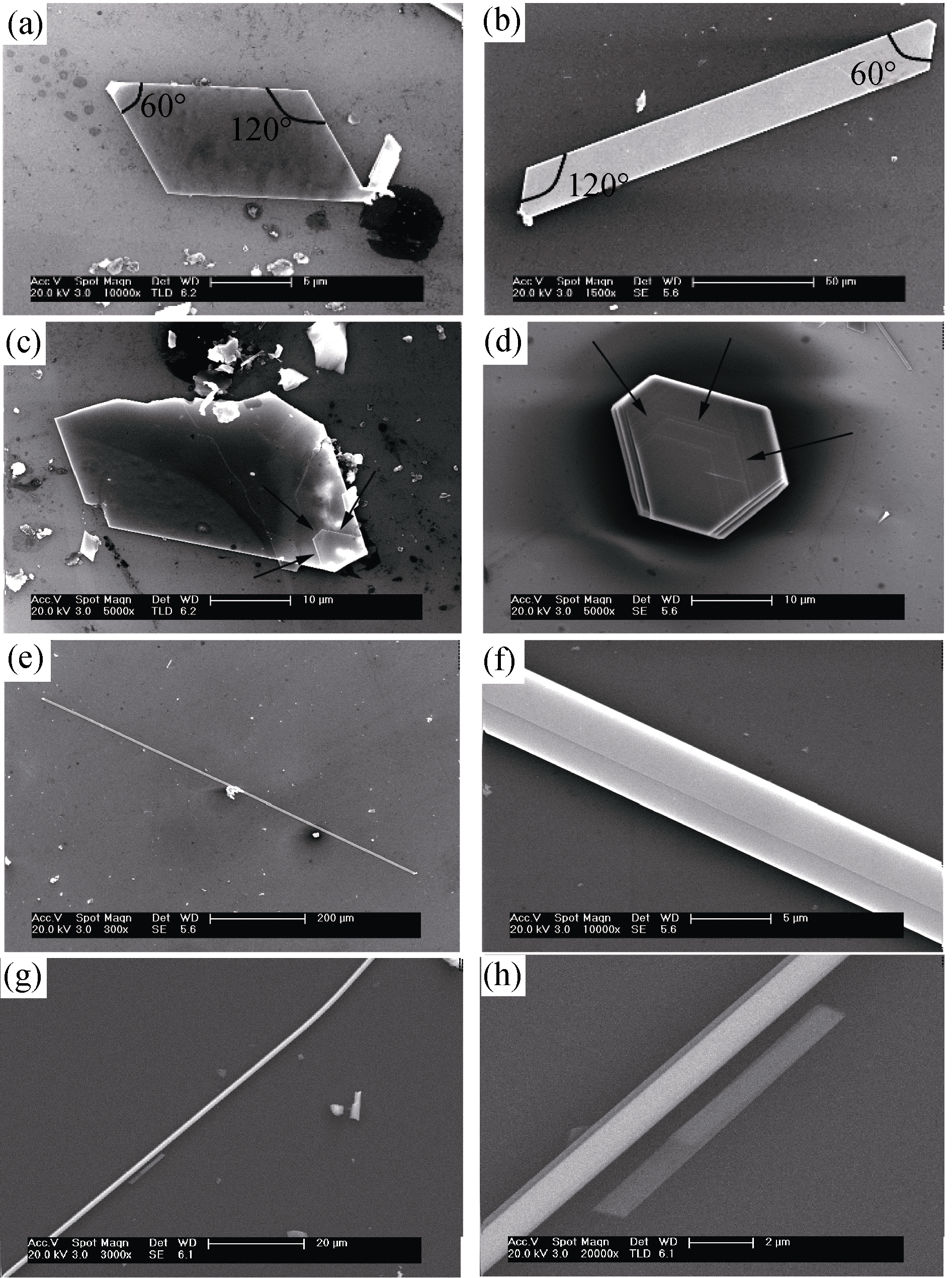
Fig. 6 SEM images of Bi2Se3 nanoplates (a-d) and Bi2Se3 nanoribbons (e-h) at different magnifications
| [1] | HICKS L D, DRESSELHAUS M S. Effect of quantum-well structures on the thermoelectric figure of merit. Phys. Rev. B, 1993, 47(19): 12727-12731. |
| [2] | HEREMANS J P, THRUSH C M, MORELLI D T. Thermopower enhancement in PbTe with Pb precipitates. J. Appl. Phys., 2005, 98: 063703-063708. |
| [3] | TEWELDEBRHAN D, GOYAL V, BALANDIN A A. Exfoliation and characterization of bismuth telluride atomic quintuples and quasi-two-dimensional crystals. Nano Lett., 2010, 10: 1209-1218. |
| [4] | QI XIAO-LIANG, ZHANG SHOU-CHENG. Topological insulators and superconductors. Rev. Mod. Phys., 2011, 83(4): 1057-1110. |
| [5] | CAO HE-LIN, XU SU-YANG, MIOTKOWSKI I, et al. Structural and electronic properties of highly doped topological insulator Bi2Se3 crystals. Phys. Status Solidi RRL, 2013, 7: 133-135. |
| [6] | ZHANG QIAN-FAN, ZHANG ZHI-YONG, ZHU ZHI-YONG, et al. Exotic topological insulator states and topological phase transitions in Sb2Se3-Bi2Se3 heterostructures. ACS Nano, 2012, 6(3): 2345-2352. |
| [7] | WANG JING, ZHU BANG-FEN. Elastic scattering of surface states on three-dimensional topological insulators. Chin. Phys. B, 2013, 22(6): 067301-067309. |
| [8] | XIU FA-XIAN, ZHAO TONG-TONG. Topological insulator nanostructures and devices. Chin. Phys. B, 2013, 22(9): 096104-096117. |
| [9] | LIU YI, MA ZHENG, ZHAO YAN-FEI, et al. Transport properties of topological insulators films and nanowires. Chin. Phys. B, 2013, 22(6): 067302-067315. |
| [10] | MIN Y, MOON G D, KIM B S, et al. Quick, controlled synthesis of ultrathin Bi2Se3 nanodiscs and nanosheets. J. Am. Chem. Soc., 2012, 134: 2872-2875. |
| [11] | CHEN Y L, CHU J H, ANALYTIS J G, et al. Massive dirac fermion on the surface of a magnetically doped topological insulator. Science, 2010, 329: 659-662. |
| [12] | KIRSHENBAUM K, SYERS P S, HOPE A P, et al. Pressure- induced unconventional superconducting phase in the topological insulator Bi2Se3. Phys. Rev. Lett., 2013, 111(8): 087001-087005. |
| [13] | KONG DE-SHENG, KOSKI K J, CHA J, et al. Ambipolar field effect in Sb-doped Bi2Se3 nanoplates by solvothermal synthesis. Nano Lett., 2013, 13: 632-636. |
| [14] | PENG HAI-LIN, LAI KE-JI, KONG DE-SHENG, et al. Aharonov- Bohm interference in topological insulator nanoribbons. Nat. Mater, 2010, 9: 225-229. |
| [15] | ZHANG YI, HE KE, CHANG CUI-ZU, et al. Crossover of the three-dimensional topological insulator Bi2Se3 to the two- dime-nsional limit. Nat. Phys., 2010, 6: 584-588. |
| [16] | ZHANG GEN-QIANG, WANG WEI, LU XIAO-LI, et al. Solvothermal synthesis of Ⅴ-Ⅵ binary and ternary hexagonal platelets: the oriented attachment mechanism. Cryst. Growth Des., 2009, 9(1): 145-150. |
| [17] | SUN ZHENG-LIANG, CONG SHENG, FU LIU, et al. A general strategy to bismuth chalcogenide films by chemical vapor transport. J. Mater. Chem., 2011, 21: 2351-2355. |
| [18] | CHEN XI, MA XU-CUN, HE KE, et al. Molecular beam epitaxial growth of topological insulators. Adv. Mater., 2011, 23: 1162-1165. |
| [19] | XIE MAO-HAI, GUO XIN, XU ZHONG-JIE, et al. Molecular-beam epitaxy of topological insulator Bi2Se3 (111) and (221) thin films. Chin. Phys. B, 2013, 22(6): 068101-068108. |
| [20] | KONG DE-SHENG, DANG WEN-HUI, J. CHA J, et al. Few-layer nanoplates of Bi2Se3 and Bi2Te3 with highly tunable chemical potential. Nano Lett., 2010, 10: 2245-2250. |
| [21] | ZHAO YI-MIN, HUGHES R W, SU ZI-XUE, et al. One-step synthesis of bismuth telluride nanosheets of a few quintuple layers in thickness. Angew. Chem. Int. Ed., 2011, 50: 10397-10401. |
| [22] | LI HUI, CAO JIE, ZHENG WEN-SHAN, et al. Controlled synthesis of topological insulator nanoplate arrays on mica. J. Am. Chem. Soc., 2012, 134: 6132-6135. |
| [23] | KIM T H, BAECK J H, CHOI H, et al. Phase transformation of alternately layered Bi/Se structure to well-ordered single crystalline Bi2Se3 structures by a self-organized ordering process. J. Phys. Chem. C, 2012, 116: 3737-3746. |
| [24] | DANG WEN-HUI, PENG HAI-LIN, LI HUI, et al. Epitaxial heterostructures of ultrathin topological insulator nanoplate and graphene. Nano Lett., 2010, 10: 2870-2876. |
| [25] | ZHANG JUN, PENG ZE-PING, SONI A, et al. Raman spectroscopy of few-quintuple layer topological insulator Bi2Se3 nanoplatelets. Nano Lett., 2011, 11: 2407-2414. |
| [26] | SONI A, ZHAO YAN-YUAN, YU LI-GEN, et al. Enhanced thermoelectric properties of solution grown Bi2Te3-xSex nanoplatelet composites. Nano Lett., 2012, 12: 1203-1209. |
| [27] | LIU H W, YUAN H T, FUKUI N, et al. Growth of topological insulator Bi2Te3 ultrathin films on Si (111) investigated by low-energy electron microscopy. Crystal Growth & Design, 2010, 10(10): 4491-4493 |
| [28] | CHA J J, KOSKI K J, CUI Y. Topological insulator nanostructures. Phys. Status Solidi RRL, 2013, 7: 15-25. |
| [29] | KOSKI K J, WESSELLS C D, REED B W, et al. Chemical intercalation of zerovalent metals into 2D layered Bi2Se3 nanoribbons. J. Am. Chem. Soc, 2012, 134: 13773-13779. |
| [30] | YAN YUAN, LIAO ZHI-MIN, ZHOU YANG-BO, et al. Synthesis and quantum transport properties of Bi2Se3 topological insulator nanostructures. Nature, 2013, 3: 1264-1268. |
| [1] | CHEN Xiangjie, LI Ling, LEI Tianfu, WANG Jiajia, WANG Yaojin. Enhanced Piezoelectric Properties of (1-x)(0.8PZT-0.2PZN)-xBZT Ceramics via Phase Boundary and Domain Engineering [J]. Journal of Inorganic Materials, 2025, 40(6): 729-734. |
| [2] | SU Haojian, ZHOU Min, LI Laifeng. Optimization of Thermoelectric Properties of SnTe via Multi-element Doping [J]. Journal of Inorganic Materials, 2024, 39(10): 1159-1166. |
| [3] | ZHANG Zhimin, GE Min, LIN Han, SHI Jianlin. Novel Magnetoelectric Catalytic Nanoparticles: RNS Release and Antibacterial Efficiency [J]. Journal of Inorganic Materials, 2024, 39(10): 1114-1124. |
| [4] | ZHAO Yawen, QU Fajin, WANG Yanyi, WANG Zhiwen, CHEN Chusheng. Preparation and Properties of Aluminum Silicate Fiber Supported PtTFPP-PDMS Flexible Oxygen Sensing Components [J]. Journal of Inorganic Materials, 2024, 39(10): 1084-1090. |
| [5] | SHEN Hao, CHEN Qianqian, ZHOU Boxiang, TANG Xiaodong, ZHANG Yuanyuan. Preparation and Energy Storage Properties of A-site La/Sr Co-doped PbZrO3 Thin Films [J]. Journal of Inorganic Materials, 2024, 39(9): 1022-1028. |
| [6] | CHENG Jun, ZHANG Jiawei, QIU Pengfei, CHEN Lidong, SHI Xun. Preparation and Thermoelectric Transport Properties of P-doped β-FeSi2 [J]. Journal of Inorganic Materials, 2024, 39(8): 895-902. |
| [7] | HUANG Jie, WANG Liuying, WANG Bin, LIU Gu, WANG Weichao, GE Chaoqun. Research Progress on Modulation of Electromagnetic Performance through Micro-nanostructure Design [J]. Journal of Inorganic Materials, 2024, 39(8): 853-870. |
| [8] | ZHENG Bin, KANG Kai, ZHANG Qing, YE Fang, XIE Jing, JIA Yan, SUN Guodong, CHENG Laifei. Preparation and Thermal Stability of Ti3SiC2 Ceramics by Polymer Derived Ceramics Method [J]. Journal of Inorganic Materials, 2024, 39(6): 733-740. |
| [9] | CHEN Hao, FAN Wenhao, AN Decheng, CHEN Shaoping. Improvement of Thermoelectric Performance of SnTe by Energy Band Optimization and Carrier Regulation [J]. Journal of Inorganic Materials, 2024, 39(3): 306-312. |
| [10] | DENG Shungui, ZHANG Chuanfang. MXene Multifunctional Inks: a New Perspective toward Printable Energy-related Electronic Devices [J]. Journal of Inorganic Materials, 2024, 39(2): 195-203. |
| [11] | ZHANG Ruiyang, WANG Yi, OU Bowen, ZHOU Ying. α-Ni(OH)2 Surface Hydroxyls Synergize Ni3+ Sites for Catalytic Formaldehyde Oxidation [J]. Journal of Inorganic Materials, 2023, 38(10): 1216-1222. |
| [12] | WANG Bo, YU Jian, LI Cuncheng, NIE Xiaolei, ZHU Wanting, WEI Ping, ZHAO Wenyu, ZHANG Qingjie. Service Stability of Gd/Bi0.5Sb1.5Te3 Thermo-electro-magnetic Gradient Composites [J]. Journal of Inorganic Materials, 2023, 38(6): 663-670. |
| [13] | QI Zhanguo, LIU Lei, WANG Shouzhi, WANG Guogong, YU Jiaoxian, WANG Zhongxin, DUAN Xiulan, XU Xiangang, ZHANG Lei. Progress in GaN Single Crystals: HVPE Growth and Doping [J]. Journal of Inorganic Materials, 2023, 38(3): 243-255. |
| [14] | YU Ruixian, WANG Guodong, WANG Shouzhi, HU Xiaobo, XU Xiangang, ZHANG Lei. Effect of High-temperature Annealing on AlN Crystal Grown by PVT Method [J]. Journal of Inorganic Materials, 2023, 38(3): 343-349. |
| [15] | ZHANG Wenjun, ZHAO Xueying, LÜ Jiangwei, QU Youpeng. Progresses on Hollow Periodic Mesoporous Organosilicas: Preparation and Application in Tumor Therapy [J]. Journal of Inorganic Materials, 2022, 37(11): 1192-1202. |
| Viewed | ||||||
|
Full text |
|
|||||
|
Abstract |
|
|||||