| [1] |
HICKS L D, DRESSELHAUS M S. Effect of quantum-well structures on the thermoelectric figure of merit. Phys. Rev. B, 1993, 47(19): 12727-12731.
|
| [2] |
HEREMANS J P, THRUSH C M, MORELLI D T. Thermopower enhancement in PbTe with Pb precipitates. J. Appl. Phys., 2005, 98: 063703-063708.
|
| [3] |
TEWELDEBRHAN D, GOYAL V, BALANDIN A A. Exfoliation and characterization of bismuth telluride atomic quintuples and quasi-two-dimensional crystals. Nano Lett., 2010, 10: 1209-1218.
|
| [4] |
QI XIAO-LIANG, ZHANG SHOU-CHENG. Topological insulators and superconductors. Rev. Mod. Phys., 2011, 83(4): 1057-1110.
|
| [5] |
CAO HE-LIN, XU SU-YANG, MIOTKOWSKI I, et al. Structural and electronic properties of highly doped topological insulator Bi2Se3 crystals. Phys. Status Solidi RRL, 2013, 7: 133-135.
|
| [6] |
ZHANG QIAN-FAN, ZHANG ZHI-YONG, ZHU ZHI-YONG, et al. Exotic topological insulator states and topological phase transitions in Sb2Se3-Bi2Se3 heterostructures. ACS Nano, 2012, 6(3): 2345-2352.
|
| [7] |
WANG JING, ZHU BANG-FEN. Elastic scattering of surface states on three-dimensional topological insulators. Chin. Phys. B, 2013, 22(6): 067301-067309.
|
| [8] |
XIU FA-XIAN, ZHAO TONG-TONG. Topological insulator nanostructures and devices. Chin. Phys. B, 2013, 22(9): 096104-096117.
|
| [9] |
LIU YI, MA ZHENG, ZHAO YAN-FEI, et al. Transport properties of topological insulators films and nanowires. Chin. Phys. B, 2013, 22(6): 067302-067315.
|
| [10] |
MIN Y, MOON G D, KIM B S, et al. Quick, controlled synthesis of ultrathin Bi2Se3 nanodiscs and nanosheets. J. Am. Chem. Soc., 2012, 134: 2872-2875.
|
| [11] |
CHEN Y L, CHU J H, ANALYTIS J G, et al. Massive dirac fermion on the surface of a magnetically doped topological insulator. Science, 2010, 329: 659-662.
|
| [12] |
KIRSHENBAUM K, SYERS P S, HOPE A P, et al. Pressure- induced unconventional superconducting phase in the topological insulator Bi2Se3. Phys. Rev. Lett., 2013, 111(8): 087001-087005.
|
| [13] |
KONG DE-SHENG, KOSKI K J, CHA J, et al. Ambipolar field effect in Sb-doped Bi2Se3 nanoplates by solvothermal synthesis. Nano Lett., 2013, 13: 632-636.
|
| [14] |
PENG HAI-LIN, LAI KE-JI, KONG DE-SHENG, et al. Aharonov- Bohm interference in topological insulator nanoribbons. Nat. Mater, 2010, 9: 225-229.
|
| [15] |
ZHANG YI, HE KE, CHANG CUI-ZU, et al. Crossover of the three-dimensional topological insulator Bi2Se3 to the two- dime-nsional limit. Nat. Phys., 2010, 6: 584-588.
|
| [16] |
ZHANG GEN-QIANG, WANG WEI, LU XIAO-LI, et al. Solvothermal synthesis of Ⅴ-Ⅵ binary and ternary hexagonal platelets: the oriented attachment mechanism. Cryst. Growth Des., 2009, 9(1): 145-150.
|
| [17] |
SUN ZHENG-LIANG, CONG SHENG, FU LIU, et al. A general strategy to bismuth chalcogenide films by chemical vapor transport. J. Mater. Chem., 2011, 21: 2351-2355.
|
| [18] |
CHEN XI, MA XU-CUN, HE KE, et al. Molecular beam epitaxial growth of topological insulators. Adv. Mater., 2011, 23: 1162-1165.
|
| [19] |
XIE MAO-HAI, GUO XIN, XU ZHONG-JIE, et al. Molecular-beam epitaxy of topological insulator Bi2Se3 (111) and (221) thin films. Chin. Phys. B, 2013, 22(6): 068101-068108.
|
| [20] |
KONG DE-SHENG, DANG WEN-HUI, J. CHA J, et al. Few-layer nanoplates of Bi2Se3 and Bi2Te3 with highly tunable chemical potential. Nano Lett., 2010, 10: 2245-2250.
|
| [21] |
ZHAO YI-MIN, HUGHES R W, SU ZI-XUE, et al. One-step synthesis of bismuth telluride nanosheets of a few quintuple layers in thickness. Angew. Chem. Int. Ed., 2011, 50: 10397-10401.
|
| [22] |
LI HUI, CAO JIE, ZHENG WEN-SHAN, et al. Controlled synthesis of topological insulator nanoplate arrays on mica. J. Am. Chem. Soc., 2012, 134: 6132-6135.
|
| [23] |
KIM T H, BAECK J H, CHOI H, et al. Phase transformation of alternately layered Bi/Se structure to well-ordered single crystalline Bi2Se3 structures by a self-organized ordering process. J. Phys. Chem. C, 2012, 116: 3737-3746.
|
| [24] |
DANG WEN-HUI, PENG HAI-LIN, LI HUI, et al. Epitaxial heterostructures of ultrathin topological insulator nanoplate and graphene. Nano Lett., 2010, 10: 2870-2876.
|
| [25] |
ZHANG JUN, PENG ZE-PING, SONI A, et al. Raman spectroscopy of few-quintuple layer topological insulator Bi2Se3 nanoplatelets. Nano Lett., 2011, 11: 2407-2414.
|
| [26] |
SONI A, ZHAO YAN-YUAN, YU LI-GEN, et al. Enhanced thermoelectric properties of solution grown Bi2Te3-xSex nanoplatelet composites. Nano Lett., 2012, 12: 1203-1209.
|
| [27] |
LIU H W, YUAN H T, FUKUI N, et al. Growth of topological insulator Bi2Te3 ultrathin films on Si (111) investigated by low-energy electron microscopy. Crystal Growth & Design, 2010, 10(10): 4491-4493
|
| [28] |
CHA J J, KOSKI K J, CUI Y. Topological insulator nanostructures. Phys. Status Solidi RRL, 2013, 7: 15-25.
|
| [29] |
KOSKI K J, WESSELLS C D, REED B W, et al. Chemical intercalation of zerovalent metals into 2D layered Bi2Se3 nanoribbons. J. Am. Chem. Soc, 2012, 134: 13773-13779.
|
| [30] |
YAN YUAN, LIAO ZHI-MIN, ZHOU YANG-BO, et al. Synthesis and quantum transport properties of Bi2Se3 topological insulator nanostructures. Nature, 2013, 3: 1264-1268.
|
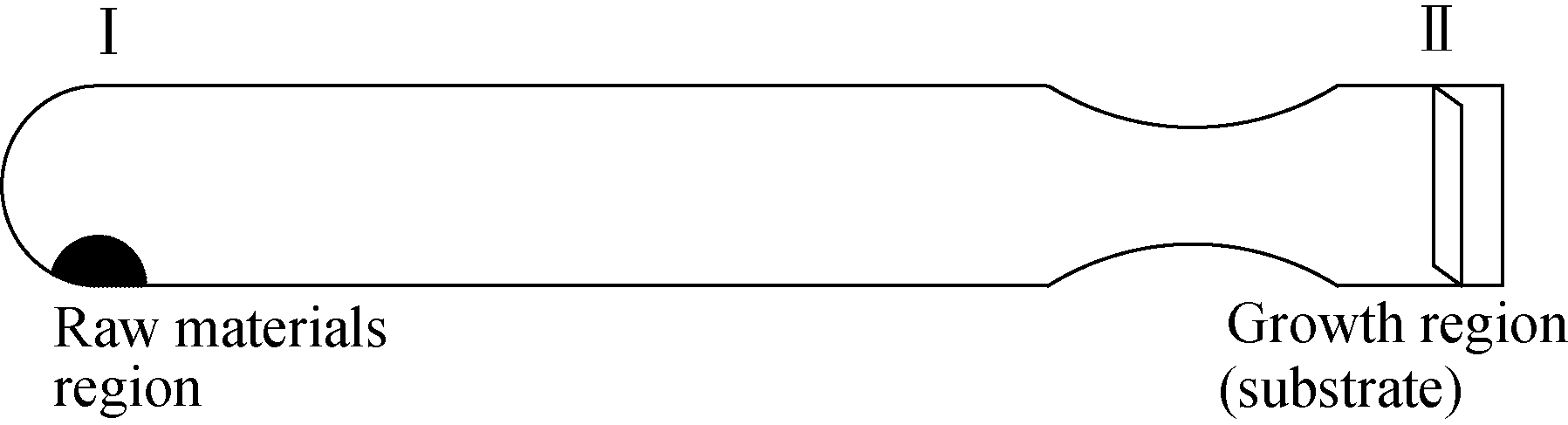
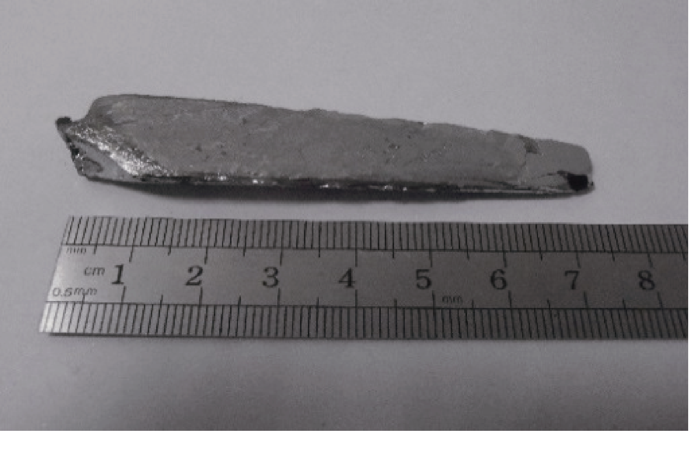
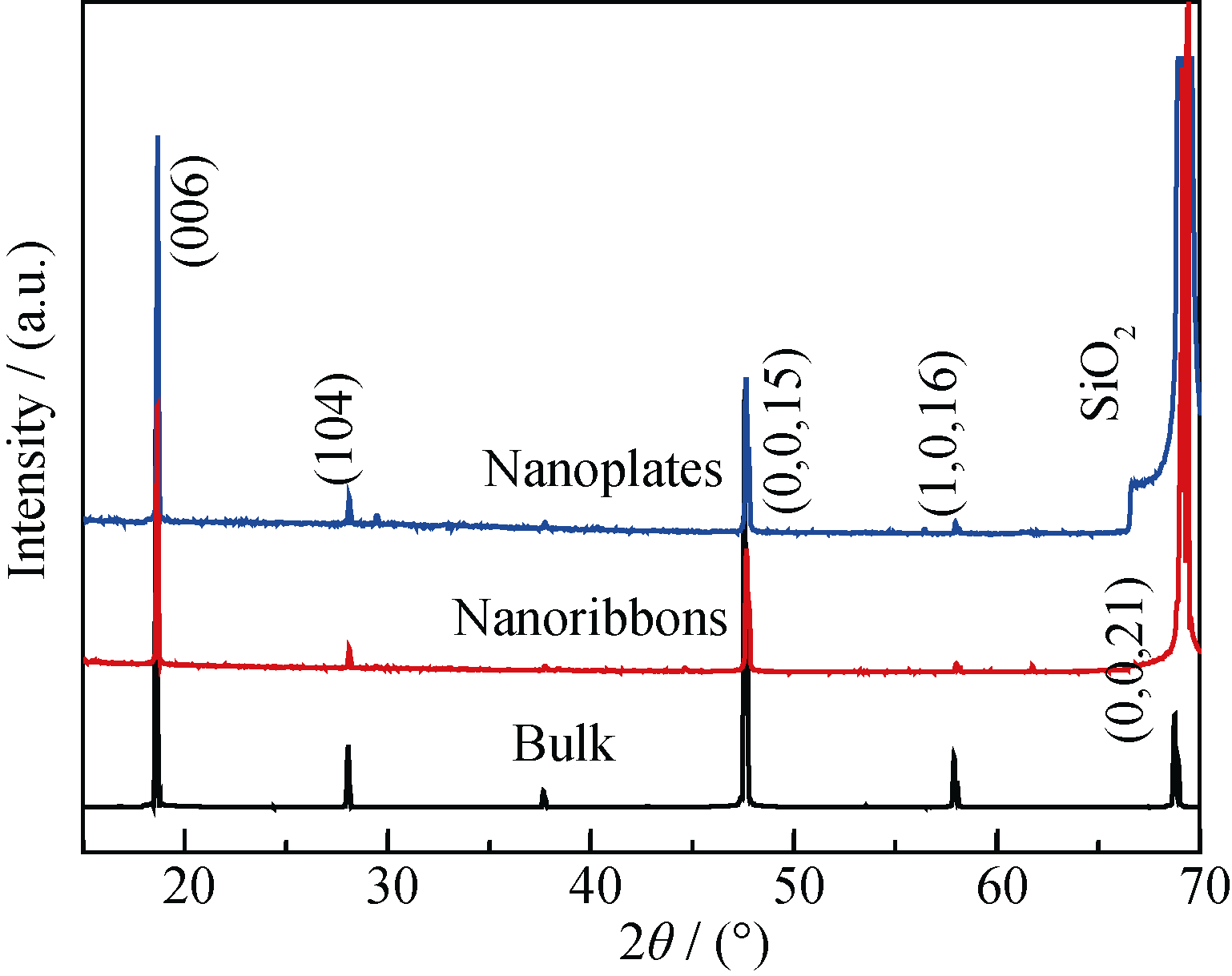
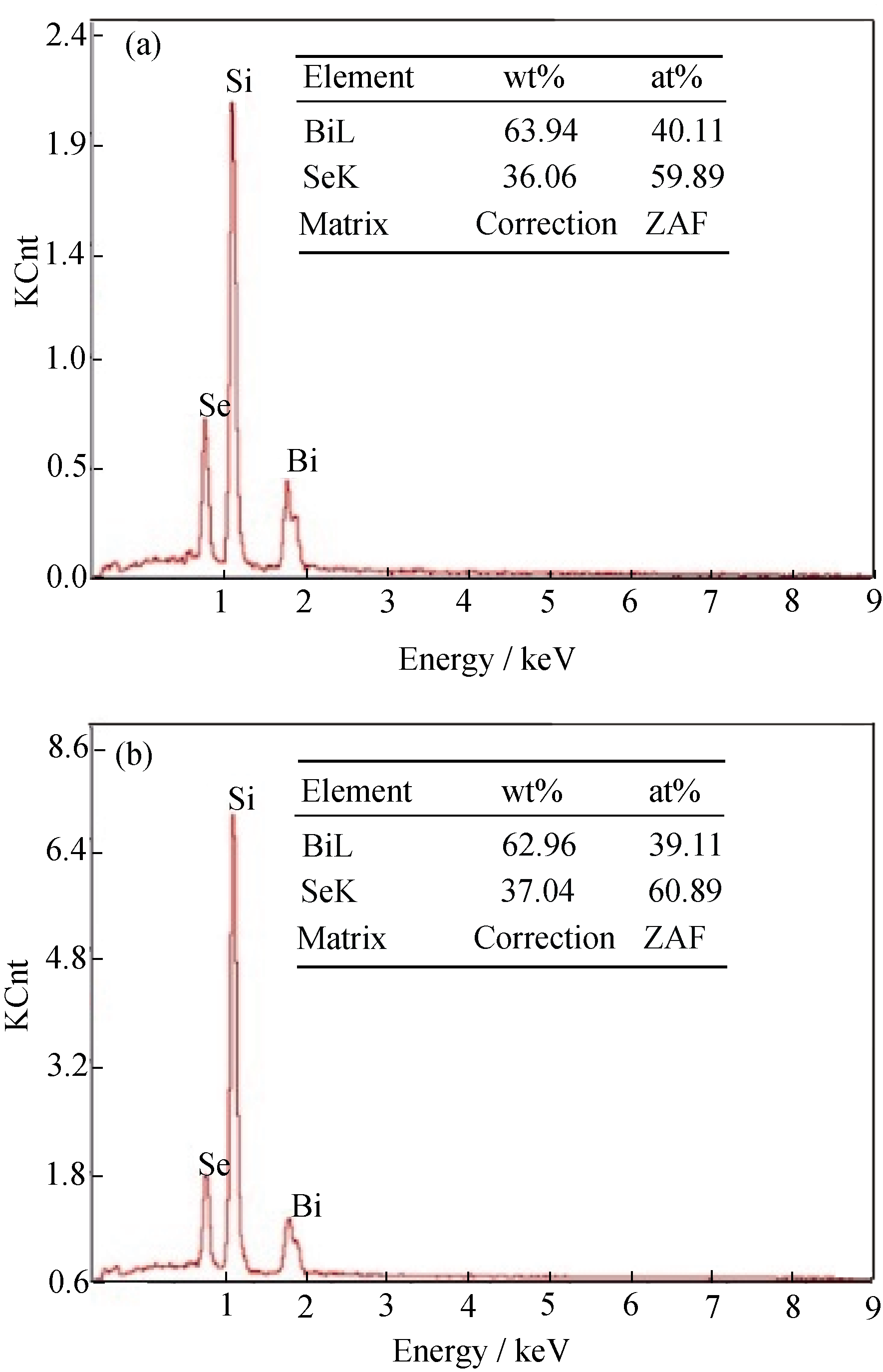
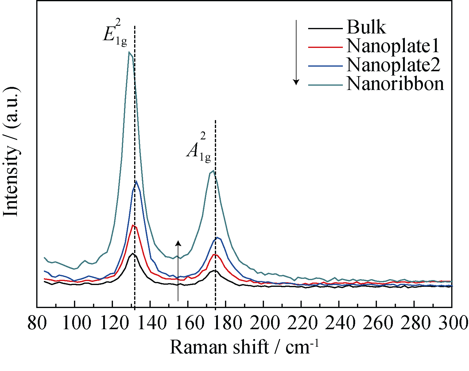
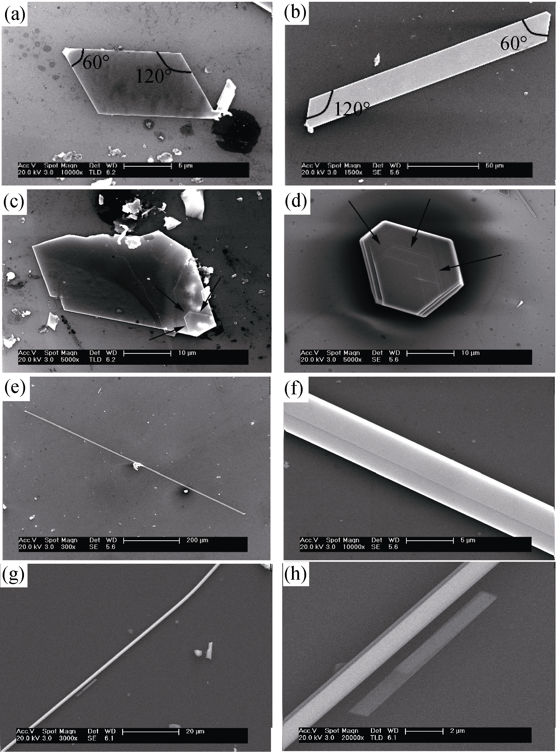
 方向生长速度快, 生成大尺寸单晶Bi2Se3纳米片; 在较低温度下, 沿
 方向生长速度快, 生成大尺寸单晶Bi2Se3纳米带。这些研究结果完善了大尺寸Bi2Se3纳米材料的制备工艺, 有望在微电子器件领域得到商业化应用。